
You are using an out of date browser. It may not display this or other websites correctly.
You should upgrade or use an alternative browser.
You should upgrade or use an alternative browser.
low inductance output stage contruction
- Thread starter Lebowski
- Start date
Lebowski
10 MW
Thanks for the offer of the tape, Hotrod, but I think it will be of little use. The copper I use is from a sheet and
warps when you cut it. So it is kinda flat but not perfectly so. No use to spend money to have them separated
0.01mm... what I'll do is put the output stage together with the busbars touching, and then when it's completed
I'll wiggle some baking paper (backpapier) between the two copper busbars.
warps when you cut it. So it is kinda flat but not perfectly so. No use to spend money to have them separated
0.01mm... what I'll do is put the output stage together with the busbars touching, and then when it's completed
I'll wiggle some baking paper (backpapier) between the two copper busbars.
Futterama
1 kW
Lebowski,
I just read through your first posts in this thread and suddenly I understood it!
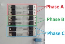
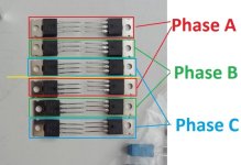
So, in the post where you mention a 12 FET compared to 2 single 6 FET, the 12 FET on a single busbar could be arranged in 2 ways, see my pictures.
In the second picture, imagine that the busbar is seperated at the yellow line and connected by wire in a star fashion as mentioned. Is this not the exact same thing as letting the busbar be one long piece? Or at least if the power wires are connected in the middle where the yellow line is instead of at the end of the busbar.
I just read through your first posts in this thread and suddenly I understood it!
So, in the post where you mention a 12 FET compared to 2 single 6 FET, the 12 FET on a single busbar could be arranged in 2 ways, see my pictures.
In the second picture, imagine that the busbar is seperated at the yellow line and connected by wire in a star fashion as mentioned. Is this not the exact same thing as letting the busbar be one long piece? Or at least if the power wires are connected in the middle where the yellow line is instead of at the end of the busbar.
Attachments
Lebowski
10 MW
In the second picture, I would be afraid for un-even current distribution. I would be afraid the
middle phase A and C FETs would conduct significantly more current than the ones on the outside.
I don't know whether my fear is justified but splitting the whole thing into two separate 6 FETs
will, at first glance, avoid this problem.
middle phase A and C FETs would conduct significantly more current than the ones on the outside.
I don't know whether my fear is justified but splitting the whole thing into two separate 6 FETs
will, at first glance, avoid this problem.
Futterama
1 kW
But Lebowski, if you seperate the 12 FET in the second picture, you get two 6 FET, but then you connect them with a wire the same place you just cut the busbar. To me, it seems like it's the same thing.
Lebowski
10 MW
Futterama said:But Lebowski, if you seperate the 12 FET in the second picture, you get two 6 FET, but then you connect them with a wire the same place you just cut the busbar. To me, it seems like it's the same thing.
Yeah but you make 'm star connected (so parallel to a common point), while what you suggest is series connected...
Futterama
1 kW
Did you see my picture where I split it up? If that is series connected, then you have to show me the parallel connection cause I can't image it then.Lebowski said:Yeah but you make 'm star connected (so parallel to a common point), while what you suggest is series connected...
Lebowski
10 MW
Ah, I missed the picture  But that's exactly the situation of my picture, no ? I only drew the wires longer for clarity...

Anyway, I am still thinking about a comment from I think HH, maybe some inductance in the power supply wire going to each individual
stage would be a good thing, it helps the case where for instance some current from phase A in one 6FET wants to go out via
the B and C of another 6 FET... one long busbar with an in the middle supply connection would then not be so good...
Futterama
1 kW
Yes, that's what I mean, you could keep the longer busbars for a 12 FET but only if the FETs are arranged properly and the power wires attach in the middle so you essentially get 2 seperate 6 FET that's connected in star using the busbar.
Futterama
1 kW
In what kind of situation would that happen?Lebowski said:...maybe some inductance in the power supply wire going to each individual stage would be a good thing, it helps the case where for instance some current from phase A in one 6FET wants to go out via the B and C of another 6 FET...
Lebowski
10 MW
Tja, I got the feeling Murphy has a big interest in ebikes, his law seems to apply everywhere.Futterama said:In what kind of situation would that happen?Lebowski said:...maybe some inductance in the power supply wire going to each individual stage would be a good thing, it helps the case where for instance some current from phase A in one 6FET wants to go out via the B and C of another 6 FET...
The unequal current sharing is possible in theory so it'll probably happen. Inductance in the lines to
the common power star-point will help to prevent it, so having some is a good thing.
Just looked again at your picture, I would swap one of the 6 FETs such that both have phase A close
to the power point and phase C furthest away...
Lebowski
10 MW
I posted this in another thread but want to repeat it here as it's more appropriate.
Attached are the Kicad database (schematic and board layout) and Gerber files for the PCB I want to use
with the output stage discussed in the first post of this thread.
The PCB contains my controller IC, room for 6 output stage drivers driving 24 FETs in total (so 4 6FET sections),
and a power supply capable of providing the necessary 15V and 5V from the battery voltage (I plan to use
upto 120 V).
Attachments
Futterama
1 kW
In my round design, the 3 low side FETs are sitting right next to each other, and so do the 3 high side FETs. The inductance I tried to calculate here: http://endless-sphere.com/forums/viewtopic.php?p=848585#p848585Lebowski said:Tja, I got the feeling Murphy has a big interest in ebikes, his law seems to apply everywhere.
The unequal current sharing is possible in theory so it'll probably happen. Inductance in the lines to
the common power star-point will help to prevent it, so having some is a good thing.
is inductance from the power wires (common star-point) to each of the 3-pair FETs. So my design basically has very little inductance between the FETs, both because they are located close together and because the busbar is slightly thinner here to allow room for the FETs, and my design also have some inductance between each FET-phase-pair and the common star-point. I think I need to draw this

For equal resistance and inductance in the busbar, yes, I see why you mention this.Lebowski said:Just looked again at your picture, I would swap one of the 6 FETs such that both have phase A close
to the power point and phase C furthest away...
h0tr0d
1 kW
- Joined
- Apr 28, 2012
- Messages
- 460
Lebowski said:It will however not solve the higher inductance you get when making the whole
structure longer for parallelling FETs. You still have all the motor currents running
between the phase wires, first in one copper busbar plate and all switching over to
the othe busbar plate in the other half of the PWM cycle. The caps don't help against
this, however artfully you arrange them.
I think we disagree on this Lebo. IMO, the caps do help a lot, specially if positioned like NJay's picture shows. If there's a voltage spike, the cap will absorb that energy IF the inductive path to the cap is low, which is dependent of geometry of path, distance and lastly ESL of the cap.
Try NJay's suggestion.
Or better still, put some MLCC in the red areas:

liveforphysics
100 TW
With respect to cap placement, and balanced inductance layout, you will notice on the new IXYS triple phase-leg modules give you the input high current leads in 3 separate sections with even spacing adjacent from each bridge's output pins. Most triple phase-leg modules before this generation just have a single power input point, which makes it almost impossible to balance inductance. It seems industry is picking up on the design advantages (cap placement options, balanced paths, etc) we're discussing in this thread.
http://ixapps.ixys.com/DataSheet/MTI145WX100GC.pdf
http://ixapps.ixys.com/DataSheet/MTI145WX100GC.pdf
h0tr0d
1 kW
- Joined
- Apr 28, 2012
- Messages
- 460
liveforphysics said:Most triple phase-leg modules before this generation just have a single power input point, which makes it almost impossible to balance inductance. It seems industry is picking up on the design advantages (cap placement options, balanced paths, etc) we're discussing in this thread.
http://ixapps.ixys.com/DataSheet/MTI145WX100GC.pdf
100% agreed. That's why i've posted those controller photos (good-ish cap location and bus bar geometry) and was advising Lebo to put some nice capacitance "really close" (aka low inductance path) to the FET's.
Or how about something like this... For a little more....liveforphysics said:With respect to cap placement, and balanced inductance layout, you will notice on the new IXYS triple phase-leg modules give you the input high current leads in 3 separate sections with even spacing adjacent from each bridge's output pins. Most triple phase-leg modules before this generation just have a single power input point, which makes it almost impossible to balance inductance. It seems industry is picking up on the design advantages (cap placement options, balanced paths, etc) we're discussing in this thread.
http://ixapps.ixys.com/DataSheet/MTI145WX100GC.pdf
http://www.pwrx.com/Product/PM600CLA060HighHopes
10 kW
- Joined
- Mar 28, 2013
- Messages
- 929
they sky's the limitOr how about something like this... For a little more.
Electric Eel
1 mW
- Joined
- Sep 9, 2010
- Messages
- 14
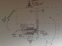
I have been wondering if stacking the fets on top of each other, back to back might make a shorter current path. You could then have a heatsink top and bottom, e.g taking your origional layout and stacking on another layer of fets upside down.
This should give a shorter current path between the paralleled fets.
(Sorry, no drawing)
I had started out imagining taking what you had, and folding it over, and conducting through the tabs might be good too, and allow for easier paralleling up of the phase banks. This would need water cooling if you stack a second bank vertically... Which is cool if you are into it 8)
I need to try putting both together to see which is more practical.
Attachments
Futterama
1 kW
I just had an idea.
The reason Lebowski is twisting the gate-source wires, is to reduce inductance. From what I know, the inductance is dependent on the loop area, the area between the conductors. So the closer the conductors, the better.
So it would be reasonable to assume that a wire with a thinner isolation is better than a wire with think isolation. What has thinner isolation than magnet wire?
So, I used some online calculators, and it seems like the inductance is the same for parallel wires and twisted wires, or that the inductance is even higher for twisted wire, is this correct? Is the twisting only for keeping the wires close together?
Twisted wire, 14.1nH/in:
http://www.eeweb.com/toolbox/twisted-pair

Parallel wire, 13.4nH/in:
http://www.eeweb.com/toolbox/parallel-wire-inductance
The reason Lebowski is twisting the gate-source wires, is to reduce inductance. From what I know, the inductance is dependent on the loop area, the area between the conductors. So the closer the conductors, the better.
So it would be reasonable to assume that a wire with a thinner isolation is better than a wire with think isolation. What has thinner isolation than magnet wire?
So, I used some online calculators, and it seems like the inductance is the same for parallel wires and twisted wires, or that the inductance is even higher for twisted wire, is this correct? Is the twisting only for keeping the wires close together?
Twisted wire, 14.1nH/in:
http://www.eeweb.com/toolbox/twisted-pair
Parallel wire, 13.4nH/in:
http://www.eeweb.com/toolbox/parallel-wire-inductance
It does seem that the only effect of twisting wires (apart from helping with common-mode noise) is to increase the length needed, which increases resistance, capaitance and inductance. It makes sense, considering the area and spacing of the (fixed length) wires doesn't change whether they are parallel or twisted.
Futterama
1 kW
Punx0r, yes, you are right about the fact that twisting them also increases wire length, so it is actually better to have them parallel. I don't expect common-mode noise to be an issue in a gate drive.
If twisting is only for keeping the wires close together, there are other ways to do that, like shrink tube or wire mesh and these methods would not increase wire length as twisting does.
Lebowski, please comment on this
If twisting is only for keeping the wires close together, there are other ways to do that, like shrink tube or wire mesh and these methods would not increase wire length as twisting does.
Lebowski, please comment on this
Lebowski
10 MW
I basically agree with you guys, closer together is better so thin twisted magnet wire is better than the thick isolated stuff i used in the first post.Futterama said:Punx0r, yes, you are right about the fact that twisting them also increases wire length, so it is actually better to have them parallel. I don't expect common-mode noise to be an issue in a gate drive.
If twisting is only for keeping the wires close together, there are other ways to do that, like shrink tube or wire mesh and these methods would not increase wire length as twisting does.
Lebowski, please comment on this
Keep in mind though, fight the battles worth fighting , this might not be the one worthwhile. The output side of the FET is way more important for FET survival...
Similar threads
- Replies
- 24
- Views
- 2,004
- Replies
- 15
- Views
- 5,337
- Replies
- 19
- Views
- 1,820
- Replies
- 44
- Views
- 4,317