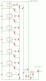
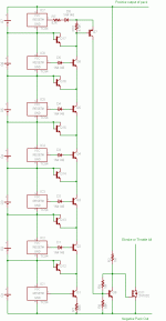
The reverse leakage currents at the lower current levels involved made me uncomfortable so I took a second pass at the design. I replaced the schottky diodes with diode connected transistors. These will have much lower leakage currents. This change required I add a diode in series with the base of each pass transistor to ensure shutoff when the output of the TC54 goes low. However all the parts are now very cheap and fairly non-critical.

The circuit operates as follows-
Assume all the battery cells are at 3V, above the 2.1V cutoff point of the TC54 ICs. This means the output of all the TC54 are high.
At the bottom stage the high output of IC1 pulls the base of Q1 to 3V, which puts about 2.4V across the emitter resistor R1 creating a pulldown current source around 16 uA out of the collector of Q1. The next highest stage IC2 output is also high and pulls the base of Q2 up through D1 to 5.5V. The 16uA current pulls down on the emitter of Q2 turning it on and the current exits out the collector to the next stage above. The transistor Q12 is connected as a diode, and is reverse biased at this point flowing no current. Each successive stage continues to pass the 16uA current along, and you can insert probably as many as 30 stages. Any more than that and you will need to have fairly high Beta transistors to minimize the current lost to the base on each stage. With a high beta transistor you could probably take it up to 100 stages. Each stage re-uses the same current as the previous stage so quiescent current consumption does not increase with added stages.
Finally the 16ua pulldown current reaches the base of the PNP Q7 pulling it down and turning it on. Because Q7 is configured as an emitter follower the base is pulled negative until Q17 starts to conduct and clamps it to one diode drop below the ground of IC7. The output of IC7 is high and pulls R7 up to the cell voltage, 3V above IC7 ground. This puts 3V minus the diode drop of D6 across R7 and the 120uA flowing through it exits out of the collector of Q7 becoming a 120uA pullup current source which turns the output FETs on.
Now say IC2 detects a low cell voltage of 2.1V and it's output goes low. This removes the base drive from Q2 and the emitter of Q2 is pulled down by the 16ua current until diode connected Q12 starts to conduct and clamps the emitter voltage of Q2 at one diode drop below the ground of IC2. This keeps Q2 off since we have the extra diode drop of D1 in series with the base of Q2. This process shunts the 16uA current off into Q12. There is now no current pulling down on the base of the PNP Q7 and it turns off. R10 shunts any residual leakage currents and keeps them from turning on Q7. This same process works for any stage.
If the top stage IC7 detects a low cell voltage and pulls it's output low it also shuts off Q7 in a somewhat similar manner.
At this point you could just put in the 12V zener D7 to clamp the gate voltage and the pulldown R8 and connect it directly to the gate of the IRB4110.
However the turn on and off times would be quite slow, especially the turn off because of the very large gate capacitance of Q11. It's a bad idea to turn the output FET on or off slowly under heavy load as the power dissipation in the FET will be enormously high during the transition. With a 1000W load the FET will be dissipating 500W in the midst of the transition. A fast transition minimizes the time for the FET to heat up. To accelerate the turn on and off times I've added Q8-Q10 and associate components
To accelerate the turn on time Q8 is connected as an emitter follower to drive the gate. It amplifies the 120uA pullup current by it's Beta so for a beta of 100 the gate pullup current will be 12ma. It may be useful to use a darlington transistor for Q8 which would give you gate turn on currents more in the 0.5-1.0A range making the gate turn on under 1 uSec.
To accelerate the turn off Q9, Q10, D8, and R9 are configured in a positive feedback clamping circuit similar to an SCR. When Q8 is pulled high current flows through D8 and charges up the gate of Q11. As long as Q8 is on and pulls up R9 and the base of Q10, Q10 remains off (and thus also Q9). However when Q7 turns off Q8 also turns off and R9 now pulls the base of Q10 down and turns it on. The collector current of Q10 flows into the base of Q9 turning it on and the collector of Q9 pulls down even harder on the base of Q10 in a positive feedback loop. This rapidly discharges the gate capacitance of Q11 through the emitter of Q10 and slams it to ground. Once the gate voltage falls below 1V the SCR circuit stops conducting and it's ready to be pulled high again by Q8.
In this second pass I've gotten rid of the schottky diodes and some unneeded parts. All the parts are fairly non-critical. Just about any small signal transistor with decent beta at low Ic can be used for Q1-Q6, Q12-Q17. A beta of over 100 at 10uA would be good, 2N5962, 2N5088, 2N5089 is good if you need something in a T0-92 package. Q7 is also fairly non critical and just needs to be able to take the full pack voltage, a KSA992 is rated to 120v. A 2N7051 darlington for Q8 will handle 100v, and 1.5 Amp giving fast turn on times. SS8050 for Q9 and SS8550 for Q10 are good high current and cheap parts that will give very fast turn off times. D8 can be a 1N4001-1N4007 type.
The Quiescent current of this circuit is low. At full pack voltage when the FET is on it is around 150uA, as the cell voltages drop this will drop toward about 100uA. You can reduce this current further, down to less than 50uA, but at the cost of increased switching times of the gate of Q11.
When low voltage cutoff is reached and the circuit turns off Quiescent current drops to about 10uA for those cells below the cell that tripped the circuit. For the cell that went below the 2.1V thresheld the current drain drops to 1uA (the quiescent current of the TC54). All the cells above this also have their current drain drop to 1uA. Any further cell that hits it's LVC threshold also has it's current drain reduce to 1uA.
Because of the active output drive the turn on and turn off times of the output FETs Q11 are very fast which protects Q11 from damage if it turns on or off into a heavy load.
This circuit will fully protect a pack, even if a motor controller or any other load is accidentally left on. If a discharged pack was left uncharged even for an extended time this circuit will continue to function correctly no matter how low the cell voltages fall and will not put any drain on the pack beyond the 1uA quiescent current of the TC54.


