Teardown: LithiumPros LithiumPowerPack 12v and 36v

amberwolf

Administrator
Staff member
Joined
Aug 17, 2009
Messages
42,759
Location
Phoenix, AZ, USA, Earth, Sol, Local Bubble, Orion
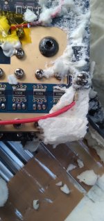
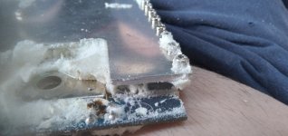
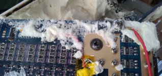
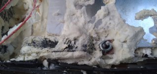
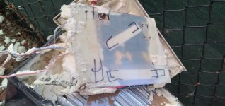
I won't get to the actual teardown for at least a few days, but Cvin dropped off these failed units for experimentation. The 12v is more swollen than the 36v, but the 36v is actually broken across the bottom of the case (probably from an impact rather than the swelling, can't tell till I get into it).

I think she said they're from around 2018. My guess is that some or all of the cells have swollen up and failed, I doubt there is compression structure in there to minimize this issue; if there is it apparently didn't work. Probably LiFePO4.

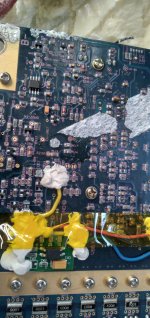
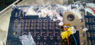
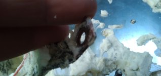
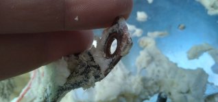
If there is a BMS it might still be good, and useful, as might any interconnects.

The casing for the 12v unit might be useful to seal up a different pack in (like for my newer trike); I think some of my EIG cells would fit inside, possibly even an entire 14s2p 52v 40Ah pack. Would be nice for the environnmental sealing. The 36v casing (cracked) might be repairable; I have a heat-tool that's designed for this kind of work to melt plastics back together (it's probably a PE type of plastic, and thus ungluable).
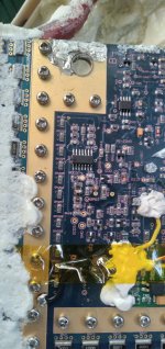
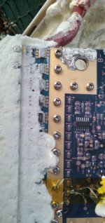
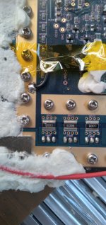
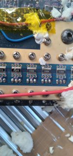
Photodump below:


20250529_224458.jpg20250529_224513.jpg20250529_224526.jpg20250529_224606.jpg20250529_224613.jpg20250529_224622.jpg20250529_224631.jpg20250529_224710.jpg
 
Had to be outside waiting on something to finish anyway, so I popped open the dead 12v pack. (which reads 0v at the terminals; I think the 36v unit reads 39v).

The body shell was cracked along one corner from the extreme swelling, pulling at the corner by tension when it wasn't designed for that. So I went ahead and just pried the top off; this broke several pieces off the top's edges, but it is still intact enough to reseal to the casing if I should decide to use it for a different battery.

It had originally been built with a foam rubber gasket between the lid and the body shell, and a clear glue that had hardened into an inflexible beaded layer had been applied to the outer face of the gray body shell where it would be overlapped by the white lid. This glue was not evenly applied, but it was present all along the entire seam gap.

The BMS is in the lid, secured there by the spray foam they filled the top of the casing with. The spray foam doesn't appear to extend all the way down all sides of the body shell and cell block inside, but I haven't attempted to extract the cell block yet (prefer not to damage it further, so considering ways to do it without cutting the body shell apart).
20250530_180540.jpg20250530_180602.jpg
There is no cell block compression mechanism, it simply has two wraps of brown plastic packing tape midway from each end to the center of the length of the cell block. This tape has stretched so much that there are clear bands in the brown. For an $1800.00 (yes, one thousand eight hundred dollar) battery, I'd expected to find good mechanical design....

There is obvious cell swelling in cells 3, 7, and 14,
20250530_183614.jpg
and cell 14 is very obviously ruptured in the middle of the edge visible once the BMS / lid was moved away.
20250530_183622.jpg

The groups from most negative to most positive read
2.24
3.29
3.129
0.677 (with the ruptured cell)

The BMS is quite complex, and is probably a good design; haven't seen one like it before.
20250530_183310.jpg
I haven't been able to locate a manufacturer or datasheet yet. One label says SB-78v6-12v-110 or 11(ohmsymbol); can't tell which, and A001 PH00 (or PHCA) 007. Another label has some chinese characters I have not been able to translate yet, then 2017/03/19, then 20171122-R12. Attempted translation has come up wiht "software" or "stylistic" or "+". Best guess is that it is the firmware revision onboard.
20250530_183304.jpg20250530_182306.jpg
It appears to have individual shunts on each FET (guessing the ones on the short edge are for charge, long edge for discharge, but haven't traced anything out yet; it's a common port BMS), so it could then monitor each individual FET and actually tell if any have failed open or shorted, if so.
20250530_182553.jpg
It also has two thermal sensors (probably tyupical thermistors) connecte dto it (one's wire tore during pack opening), but the sensors themselves were both placed within an inch of each ohter inside the sprayfoam close to the outer gray shell, nearly a centimeter from the cells, at the end of the pack opposite all the cell interconnects. Seems pretty dumb, but I don't know what they were using them for (if just for external temperature detection, that would be ok, but I'd've put one each on opposite ends, if so).
20250530_181522.jpg


It appears to be an 8S BMS (there are 8 sets of 3 parallel balance shunt resistors, and the balance/sense connector is 9 pins; it only uses six of them, two of which are connected to the same cell junction, as is common with multi-cell-configuration-compatible BMSes). The balance connector also appears to have contact oxidation or corrosion but I see no sign of water intrusion, so my guess is reaction from whatever offgassed from the sprayfoam.
20250530_180956.jpg20250530_181001.jpg
 
Thank you for posting that teardown!
Considering the price, that pack would technically be called A Piece Of Junk.
The cell handling/mounting is almost criminally negligent.

That BMS has a huge number of passives. It would be great to see the other side if not too inconvenient.
Interesting ”daughter board” bodge they got there too! Just the opto and some passives?
 
Last edited:
Thank you for posting that teardown!
I haven't seen a teardown of any of these commercially available marine / starter / etc batteries, so when the chance came to get a couple dead ones I wouldn't feel bad about destroying if it came to that.... ;)


Considering the price, that pack would technically be called A Piece Of Junk.
The cell handling/mounting is almost criminally negligent.
I think it would technically be called theft (of the buyer's presumably hard-earned cash) :lol:
But apparently these things are commonly used in all sorts of boating / etc applications successfully. I didn't search hard but I didn't find a fire involving one yet.

Hopefully they make them better now (this one's BMS is from 2017 and the pack is supposedly from about 2018 or so, so they have had plenty of time to learn and make their stuff better...though since money talks louder than engineers I wouldn't bet on it.


That BMS has a huge number of passives.

The ones that are along the edge of the board appear to be shunts (R003) for each charge/discharge FET, from the very little looking I did at it while taking the pics. The BMS is supposed to be good for 1,500Amps MCA*** (30seconds), and 100A continuous, so these must be pretty good FETs. There are 12 along each edge where the long gold traces are with screws in them, for a total of 24. Dunno which FET is used yet.

The 220 (or 022) ones in the 3x8 array appear to be the balancers, setup as 3 in parallel for each channel. I don't know offhand how much balance current that would allow, but I suspect it's not much, even for such a huge BMS.

***from a websearch: "The marine cranking ampere (MCA) rating of a battery is very similar to the CCA rating; the only difference is that while the CCA is measured at a temperature of 0°F, the MCA is measured at 0°C. All other requirements are the same — the ampere draw is for 30 seconds and the end of discharge voltage in both cases is 1.20 volts per cell. or 7.2 volts for the whole battery."

It would be great to see the other side if not too inconvenient.
Interesting ”daughter board” bodge they got there too! Just the opto and some passives?

There will be much more detail as I have time and energy to poke at it. (in the meantime the cells are out in the far shed in a metal cabinet, just in case. ;) ).

I don't know what hte opto might be for...been trying to think what might have to be isolated but still read by the BMS (id on't know if it's an analog or digital signal or what it's connected to).

The BMS is on the workbench, but since it is probably perfectly functional, I only want to work on it when I'm not exhausted (a rare condition) and likely to break something on it. That way I can use it on new cells (well, used EV cells from greentecauto probably, once I find a useful deal I can afford) whenever I get some, or on the remaining non-failed cells in this pack (if there are any--I suspect they'll all poof right up as soon as I get the block out of the shell).

I bet that this is a programmable BMS, but that's not useful info without being able to get the programming software. There's a pad marked SENS-UART at one corner of the board. and at another spot on the other end of it too, along with EN-UART and some others I can't quite make out over by the main B- terminal.

There are ohter pics I couldn't fit in the post above that are dumped in this post below. One is a red wire going to the screw post that's over by what is probably a regulator. I bet that this red wire is the positive for the first cell block, and that's what killed it--powering the BMS only from taht group drained it dead just sitting around not being charged for who knows how long. (no info about it's former life, usage, or abuse is available). I forgot to measure the voltage on that wire relative to other wires.
 

Attachments

  • 20250530_182806.jpg
    20250530_182806.jpg
    1.2 MB · Views: 3
  • 20250530_182809.jpg
    20250530_182809.jpg
    929.1 KB · Views: 2
  • 20250530_182815.jpg
    20250530_182815.jpg
    1 MB · Views: 3
  • 20250530_182817.jpg
    20250530_182817.jpg
    1.1 MB · Views: 3
  • 20250530_182820.jpg
    20250530_182820.jpg
    1.1 MB · Views: 3
  • 20250530_182823.jpg
    20250530_182823.jpg
    1 MB · Views: 2
  • 20250530_183507.jpg
    20250530_183507.jpg
    772.9 KB · Views: 2
  • 20250530_183514.jpg
    20250530_183514.jpg
    2 MB · Views: 3
  • 20250530_182803.jpg
    20250530_182803.jpg
    1.3 MB · Views: 4
  • 20250530_182800.jpg
    20250530_182800.jpg
    4 MB · Views: 3
  • 20250530_182757.jpg
    20250530_182757.jpg
    4 MB · Views: 3
  • 20250530_180553.jpg
    20250530_180553.jpg
    2 MB · Views: 3
  • 20250530_181531.jpg
    20250530_181531.jpg
    2 MB · Views: 3
  • 20250530_182309.jpg
    20250530_182309.jpg
    4 MB · Views: 3
  • 20250530_182314.jpg
    20250530_182314.jpg
    2 MB · Views: 3
  • 20250530_182318.jpg
    20250530_182318.jpg
    835.6 KB · Views: 3
  • 20250530_182415.jpg
    20250530_182415.jpg
    2 MB · Views: 1
  • 20250530_182417.jpg
    20250530_182417.jpg
    2 MB · Views: 1
  • 20250530_182510.jpg
    20250530_182510.jpg
    2 MB · Views: 1
  • 20250530_183637.jpg
    20250530_183637.jpg
    2 MB · Views: 2
Thank you @amberwolf for the extra photos. That’s a burly-looking BMS…wow.
For the resistors you noted, I agree. I’m amazed though by the number of passives in the central portion of the board. But perhaps that’s due to its age, before the high level of integration (into single chips or low chip count boards) we have now.
 
I’m amazed though by the number of passives in the central portion of the board. But perhaps that’s due to its age, before the high level of integration (into single chips or low chip count boards) we have now.
Oh, sorry, I didn't realize you were talking about the general design with all the discrete components (vs ICs). :oops:

I don't know the specific reason they did it this way, but it could've been that the functions they wanted didn't exist in available ICs yet, or maybe they needed something that wasn't possible with an IC, or whatever. Or maybe they just wanted all those nicely-labelled test points out in the open. :) I doubt I would be able to reverse engineer the board even if I had time to trace it all out and draw it up....
 
Back
Top