
Post a picture of it if you can.
You are using an out of date browser. It may not display this or other websites correctly.
You should upgrade or use an alternative browser.
You should upgrade or use an alternative browser.
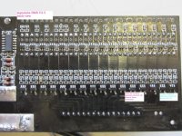
SIGNALAB (Ping) BMS Schematic
- Thread starter Niky1961
- Start date
Garycambridge
100 µW
- Joined
- Mar 2, 2011
- Messages
- 7
fixed the problem, wasn't the part I thought but for reference the 3 legged component on the front of the board is a p channel mosfet
N0100p http://www.datasheetdir.com/N0100P+download
or you can use a FDN304PZ http://uk.rs-online.com/web/search/searchBrowseAction.html?method=searchProducts&searchTerm=671-0407
N0100p http://www.datasheetdir.com/N0100P+download
or you can use a FDN304PZ http://uk.rs-online.com/web/search/searchBrowseAction.html?method=searchProducts&searchTerm=671-0407
dnmun
1 PW
there are no p channel mosfets on the ping signalab BMS.
Garycambridge
100 µW
- Joined
- Mar 2, 2011
- Messages
- 7
I thought that is was an N channel mosfet, but ping told me that it was a p channel and have put a p channel one on and its working, mine is v2.5
kafka-cloud
10 W
- Joined
- Aug 9, 2010
- Messages
- 77
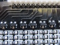
Mine melted the plastic as in the last picture in this thread. I am in the process of cleaning it up. However, does someone have a picture of the underneath of the BMS?
Cheers
Cheers
dnmun
1 PW
Garycambridge said:I thought that is was an N channel mosfet, but ping told me that it was a p channel and have put a p channel one on and its working, mine is v2.5
can you post a picture of your BMS and where this p channel FET is located. did ping tell you which mosfet to use?
Garycambridge
100 µW
- Joined
- Mar 2, 2011
- Messages
- 7
ping wrote
( Si2333 is the correct one. It should be P channel. You could also choose mi3415. Actually, you can choose any small P channel MOSFET that has more than 2amp current drain. Voltage should be more than 5v. Actually, most such MOSFETs have more than 10v. )
my electronic supplier cross referenced and said this one
FDN304PZ
http://uk.rs-online.com/web/search/sear ... m=671-0407
the original one on the board has this number and i found this on the web
N0100p
http://www.datasheetdir.com/N0100P+download
Attachments
dnmun
1 PW
ok, see if you can find them on ebay and maybe you can get a deal on them. this is good to know since the surface mounts transistors were unknown. you are missing one of the surface mount 330 ohm shunt resistors in that picture, how did that happen? that should change the shunt current by 20% too.
Garycambridge
100 µW
- Joined
- Mar 2, 2011
- Messages
- 7
well spotted, came like it, took me longer to notice, still works just takes a little longer,
I did get some parts from radio spares, but turns out that wasn't the problem anyway with send you a message about it
cheers
Gary
I did get some parts from radio spares, but turns out that wasn't the problem anyway with send you a message about it
cheers
Gary
dnmun
1 PW
like i said, post up your fix, and lemme know why that 300 ohm resistor is missing in your picture. that is the only time i have seen a surface mount part be missing after reflow. ping's inspection shoulda caught that before they used it on a battery.
Garycambridge
100 µW
- Joined
- Mar 2, 2011
- Messages
- 7
well if anybody has a LED that stays on one or more channels test if the ceramic capacitor has shorted on the back of signalabs v2.5
and unplug the BMS or it will drain that string of cells down,
heres a picture of what happened.
ceramic capacitor 250nf case style 0603
and unplug the BMS or it will drain that string of cells down,
heres a picture of what happened.
ceramic capacitor 250nf case style 0603
Attachments
dnmun
1 PW
Garycambridge said:well if anybody has a LED that stays on one or more channels test if the ceramic capacitor has shorted on the back of signalabs v2.5
and unplug the BMS or it will drain that string of cells down,
heres a picture of what happened.
ceramic capacitor 250nf case style 0603
i think we are gonna call this board an anomaly since the resistor is missing so that implies something went wrong during reflow, maybe too hot.
i can send you some of those surface mount transistors and the 330 ohm resistor if you wanna use them, i've got some parts boards here from wineboy and greg
Garycambridge
100 µW
- Joined
- Mar 2, 2011
- Messages
- 7
Cheers dnmun, but as its all working at the moment, (touch wood) will leave it alone for the time being, but thanks for the offer and keep up the good work, knew very little about this technology a few months ago and your posts have been very useful
Hi all,
looking at the schematic, what happens if the load minus is connected to the charger minus?
I mean, nothing connected to the pin "load -", both charger and load minus connected to the pin "charger -"
I think the only trouble will be on the mosfet of the overvoltage protection Q1: discharge current will flow throuth it and I'm not sure if it is dimensioned for high current, but only for lower charge current.
Maybe I can change the mosfet with a different one to withstand the higher current?
If you connect the minus sides like that, the charge current won't cut off when a cell goes too high.
The FETs are only designed to handle the charging current. Yes, you can uppgrade them. A single IRFB4110 should be able to do about 20 amps charging.
The FETs are only designed to handle the charging current. Yes, you can uppgrade them. A single IRFB4110 should be able to do about 20 amps charging.
Doctorbass
100 GW
fechter said:A single IRFB4110 should be able to do about 20 amps charging.
Totally true Fechter :wink: I'm using two in parallel for charging at up to 37 amps with my meanwell 1500W and they dont really heat alot when combined with a 2 sqrt inch area heatsink .
Doc
digitaltanha
1 µW
- Joined
- Aug 31, 2011
- Messages
- 1
My v2.5 16s signalab bms had a hot charging fet to the point of melting the solder. I took the advice of replacing it with a 75NF75. Just hooked it up to the charger about an hour ago and it seems to be working. This is the second time it has happened. The first time ping sent me a new bms. Then I stumbled across this post and figured I'd try fixing it myself.
Thanks Doctorbass and the others that contributed to coming up with this solution.
Thanks Doctorbass and the others that contributed to coming up with this solution.
Spacey
100 kW
I've just ordered some 4110 FET's as I had the same melting solder problem on charging Fet with 48V Headway Pack and Signalab BMS. Now I know why they scrape off the name on the FET's......it's so you don't see that they are so under specced and that they will fail!
58.4V Charge going into the FET, no wonder it fails, pretty sure this BMS is responsible for yet another Headway Cell breaking.
58.4V Charge going into the FET, no wonder it fails, pretty sure this BMS is responsible for yet another Headway Cell breaking.
999zip999
100 TW
Ping said that a % of fet's will fail on the signlab as that's the way it is, and the some legs have incomplete solder on the legs- QC- profits.
dnmun
1 PW
not sure why or when ping told you that you should expect the mosfets to fail. i have not noticed that all of the ping BMSs have bad mosfets, but it does seem like they get hot and if they are insulated inside there has to be the risk they will overheat. jmho
"58.4V Charge going into the FET, no wonder it fails, pretty sure this BMS is responsible for yet another Headway Cell breaking."
the charging mosfet is in the negative side of the charger leads, not the positive side. the drain is attached to the ground of the pack directly so the voltage across the mosfet when charging would be something like (2A) X (25mohm), or 50mV. doesn't seem that bad to me. how did you measure the 58..4 V across the charging mosfet?
Spacey
100 kW
I didn't measure just figured that if they are between the charger and the battery that they would have the full voltage going through them.
How on earth are they breaking at 50mv and 2A load? Mine were so hot that they came away from the PCB?
How on earth are they breaking at 50mv and 2A load? Mine were so hot that they came away from the PCB?
999zip999
100 TW
Dnmun I have had problem on a signalab bms fet's one was a poor solder on a leg's and the other was a failure. I moved on to konion's and have no bms problems so far ( human bms ).
Well, they would have full voltage across them whenever they turn off, I think, but when on, they (like phase FETs in controller) would only have the voltage created by the current flowing thru it's RDSon. So if they were say, 20milliohm FETs, and current was 2A, it'd only be 40mV across the charging FET (since it's just one, no parallelling). That's only 80mW, so there's no reason for it to get hot at all, during charging.
What might be happening is one of these things:
1--it is not melting during charge, but instead is coming off during discharge when *those* FETs heat up (though again, they shouldn't get that hot, based simply on Ohm's Law, unless they are buried inside the shrinkwrap with no airflow at all, heat trapped right there). If the other FETs got hot enough, they could heat it up enough to come off with them even though it's not in use.
2--Again, buried in teh insulation, perhaps that 80mW (maybe 100-200mW worst case with a beefier charger?) might be enough over a charge cycle ot heat it up that much.
3--The heat build up causes RDSon to rise, creating more voltage drop and thus more waste heat wattage, inside the insulated pack that then causes it to get hot enough to unsolder or fail
4--If a voltage spike during charge switchoff (HVC) kills the FET, or damages it causing even higher RDSon than usual, then #2 and 3 above would be even more likely.
Or something else I haven't thought of.
Similar threads
- Replies
- 17
- Views
- 6,190
- Replies
- 36
- Views
- 9,455
- Replies
- 64
- Views
- 15,364
- Replies
- 26
- Views
- 9,014