
Ok so TVS and regular diodes across the fets are for 2 differen purposes? I am more worried about switching lossses then stray inductance. I plan to use good caps and design to keep the stray inductance down. So does anyone have a way to calculate regular diodes? Or are tvs diodes good for this too???
You are using an out of date browser. It may not display this or other websites correctly.
You should upgrade or use an alternative browser.
You should upgrade or use an alternative browser.
Arlo's power stage Leaf controller runs and drives page 103
- Thread starter Arlo1
- Start date
Arlo1 said:Ok so TVS and regular diodes across the fets are for 2 differen purposes? I am more worried about switching lossses then stray inductance. I plan to use good caps and design to keep the stray inductance down. So does anyone have a way to calculate regular diodes? Or are tvs diodes good for this too???
Arlo, IMHO you don't need any
") . The TVS diodes clamp voltage using avalanche breakdown but the power MOSFET are designed to do exactly the same thing and handle the heat better, so they won't make a significant difference in high power application. Also, the power MOSFET already have a properly sized diode integrated, you could add more in parallel but it will increase your reverse recovery charge, delay recovery and increase switching loss...
. The TVS diodes clamp voltage using avalanche breakdown but the power MOSFET are designed to do exactly the same thing and handle the heat better, so they won't make a significant difference in high power application. Also, the power MOSFET already have a properly sized diode integrated, you could add more in parallel but it will increase your reverse recovery charge, delay recovery and increase switching loss...So there is nothing i can do mechanicaly to lower switching losses? Because as i up the pwm frequency it will become a problem....walls99 said:Arlo1 said:Ok so TVS and regular diodes across the fets are for 2 differen purposes? I am more worried about switching lossses then stray inductance. I plan to use good caps and design to keep the stray inductance down. So does anyone have a way to calculate regular diodes? Or are tvs diodes good for this too???
Arlo, IMHO you don't need any
rhitee05
10 kW
Given a particular bus voltage and phase current, the ONLY thing you can do to lower the switching losses is to switch more quickly. The switching losses are simply a function of the non-zero time it takes the FET to transition and no external components will change that. Assuming that the driver is strong enough, the main thing that will prevent you from being able to switch as quickly as you would like is inductance. Therefore, the thing to do to reduce switching losses is to reduce inductance which means very, very careful attention to layout.
A schottky diode (or multiple) in parallel with the low-side FETs can help to improve switching time slightly because they have a very fast reverse recovery, much faster than the body diode in the FETs. However, you will achieve the same result if you can minimize the inductance. Also, the only way adding a schottky will work is if you also implement synchronous rectification. It would take many diodes in parallel to handle the continuous freewheeling current (20-30 A rated each for TO-220 or similar types), but a single diode can handle brief spikes (200+ A) until the lower FET turns on and takes the current.
The purpose of TVS diodes is to absorb voltage spikes. They will not do anything to speed up switching or reduce switching losses. However, they will act to help protect the FETs against voltage spikes which may be caused by fast switching. Better to design and operate the circuit so that it's not operating close to the ragged edge, but TVS diodes might help you operate just a little bit closer. They exist for insurance and peace of mind.
salty9
1 kW
Arlo,
Tesseract had some cap recommendations in http://www.diyelectriccar.com/forums/showthread.php?t=23799&highlight=alternator+controller posts 7 and 8. There is also a thread here on the sphere in which BigMoose had similar recommendations that I couldn't find again.
Tesseract had some cap recommendations in http://www.diyelectriccar.com/forums/showthread.php?t=23799&highlight=alternator+controller posts 7 and 8. There is also a thread here on the sphere in which BigMoose had similar recommendations that I couldn't find again.
grindz145
1 MW
Just caught those water cooled boards from HK, pretty trick!
Arlo1 said:So there is nothing i can do mechanicaly to lower switching losses? Because as i up the pwm frequency it will become a problem....
I would look into different fets with smaller reverse capacitance (CRSS in datasheets), and smaller gate charge (for faster switching). Fairchilds trench-fets seems to have low gate charge and low rds'on, and low reverse capacitance.
Also, reading some buck-boost application notes will teach you something about switching losses and variables to take into calculation
Here is a comparison between 10nH and 100 nH stray inductance in the halfbridge loop. Switching frequency is 40kHz. In the first case the losses are ~20W in the lower transistor of the bridge. In the second case the losses are ~40W.
How much is 100nH inductance? Its a loop of 1.5-2 inches (~40mm) diameter/square, or thereabouts, in air.

EDIT: Attached the spice model.
How much is 100nH inductance? Its a loop of 1.5-2 inches (~40mm) diameter/square, or thereabouts, in air.
EDIT: Attached the spice model.
Attachments
Lebowski
10 MW
I'm also messing around with this now for my own power stage. I found a good paper on how to choose and dimension
snubbers. I tried the simple passive RC snubber in parallel with the FETs. This is before:
View attachment 2
this is with snubber but with no current:

this is with 3A and 600 uH inductance (and lightbulbs):

for the last image I had to change the RC values of the snubber as the extra inductance has
an impact. I only placed one which is effective in the rising edge, there is no snubber for the
falling edge.
snubbers. I tried the simple passive RC snubber in parallel with the FETs. This is before:
View attachment 2
this is with snubber but with no current:
this is with 3A and 600 uH inductance (and lightbulbs):
for the last image I had to change the RC values of the snubber as the extra inductance has
an impact. I only placed one which is effective in the rising edge, there is no snubber for the
falling edge.
Attachments
A fast "hands on" way to get a working RC snubber is this following recipe:
1. Add ceramic capacitance Cadd in parallel with switch until ringing frequency is halved. Now you know the total capacitance of the ringing circuit: C = Cadd*4/3.
2. Calculate stray inductance
f = 1 / (2*pi*sqrt(L*C)) ->
L = 1 / ((2*pi*f)^2 * C)
3. Calculate impedance of stray inductance. Z = 2*pi*f*L
4. Put a resistor of about 2*Z in series with the previously added capacitance.
The resistor needs to handle the heat. In a high power controller, it will be watts of heat.
I stole this recipe from here:
http://elektronikforumet.com/forum/viewtopic.php?f=14&t=10593
Lebowski
10 MW
I got my output stage snubbed now and I must say, the waveforms look really
clean now.
I did not completely follow the recipe as posted by bearing... I did some simplified
simulations (just an inductor, cap and the RC snubber). The higher the snubber
capacitor the better (with 3 times the parasitic cap being the minimum) as the
overshoot will reduce even more. The limit to the snubber cap is the amount
of power you're willing to dissipate
P_loss = f_pwm * C_snub * V ^ 2
I chose C=4.7nF, with 100V and 20kHz PWM this is around 1 W (which will be
dissipated not in the cap but in the snubber resistor)
With C_snubber chosen, put this cap across the drain-source of the FET to
be protected and measure the ringing frequency. Chose R_snubber such
that
R_snubber = 1.5 / (2*pi * f_ringing * C_snubber)
The 1.5 gave me the best results in the simulation but it's a broad range,
between 1 and 2 is good.
I put a snubber accross the drain-source of each of my 6 FET's, the (no current)
ringing got reduced by around a factor 10 (and is not really ringing anymore, it's
a single nicely damped overshoot)
Will post pictures here later today.
Alan B
100 GW
Excellent result!
Lebowski
10 MW
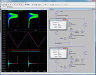
These are the with-snubber pictures, first one with no current and then one with around 4 A.
View attachment 2
If you compare this first picture with the first one of my previous post in this thread, a big improvement

You can see the snubbers across the drain-source of each FET

I build the 1W 8Ohm resistors by putting 5 0.25W 39 Ohm resistors in parallel.
Based on the power dissipation equation for the snubbers you can see the limit coming... For a simple
6 FET controller with only 20 kHz PWM you're talking 1 W per snubber (granted, at 100V supply).
An 18 FET would take 3 times as much, 60kHz PWM again 3 times as much taking you to almost
10W per snubber. By then it'll be necessary to re-read the paper I attached and to look for non-dissipative
snubbing...
View attachment 2
If you compare this first picture with the first one of my previous post in this thread, a big improvement
You can see the snubbers across the drain-source of each FET
I build the 1W 8Ohm resistors by putting 5 0.25W 39 Ohm resistors in parallel.
Based on the power dissipation equation for the snubbers you can see the limit coming... For a simple
6 FET controller with only 20 kHz PWM you're talking 1 W per snubber (granted, at 100V supply).
An 18 FET would take 3 times as much, 60kHz PWM again 3 times as much taking you to almost
10W per snubber. By then it'll be necessary to re-read the paper I attached and to look for non-dissipative
snubbing...
zombiess
10 MW
Some mighty long leads going to those FETs there Lebowski. Would shortening them up help reduce the ringing on it's own because their inductance would be reduced?
Lebowski
10 MW
zombiess said:Some mighty long leads going to those FETs there Lebowski. Would shortening them up help reduce the ringing on it's own because their inductance would be reduced?
Well what you're snubbing is the (inductance) part away from the FET and the snubber, so basically
all the interconnect to the phases and the battery (up to the first decent cap it encounters).
In my case, later I'll bend the FETs 90 deg upwards (to screw 'm to the heatsink) and
shorten the wires a bit.
rhitee05
10 kW
There's really little point to using an RC snubber on MOSFETs. The snubber serves to reduce the dv/dt when the MOSFET switches, which has the effect of slowing down the switching. You could get virtually the same effect by increasing the gate resistor, which is much simpler. Either way the ringing is decreased because the switching speed is increased, and switching losses go up.
Definitely. The only way to reduce the spikes and keep switching fast is to reduce inductance.
zombiess said:Some mighty long leads going to those FETs there Lebowski. Would shortening them up help reduce the ringing on it's own because their inductance would be reduced?
Definitely. The only way to reduce the spikes and keep switching fast is to reduce inductance.
Lebowski
10 MW
Without snubbers the ringing on the drain-source
has a peak of 150 V, with snubbers 70 V (both at 60 V supply).
I put them in to prevent the 4115's from blowing up.
has a peak of 150 V, with snubbers 70 V (both at 60 V supply).
I put them in to prevent the 4115's from blowing up.
nieles
10 kW
you could try a small (0.5-1uF) film/ceramic capacitor close to the Drain Source connection without the series connected resistor.
That will change the resonant frequency of the ringing. I don't see how it will help, unless the cap is lossy and dampens the ringing that way.nieles said:you could try a small (0.5-1uF) film/ceramic capacitor close to the Drain Source connection without the series connected resistor.
rhitee05 said:There's really little point to using an RC snubber on MOSFETs. The snubber serves to reduce the dv/dt when the MOSFET switches, which has the effect of slowing down the switching.
I don't think this is true. The purpose of the snubber is to dampen out the ringing. It's purpose is not to reduce dv/dt. I don't think it has much effect on dv/dt at all.
rhitee05
10 kW
Lebowski said:Without snubbers the ringing on the drain-source
has a peak of 150 V, with snubbers 70 V (both at 60 V supply).
I put them in to prevent the 4115's from blowing up.
You have a major inductance problem if you're getting a ringing amplitude 2.5x the supply voltage! Even with the snubber at 4 A you're getting almost 1.5x... If I were you, I'd start by making the gate resistor 2x or 3x larger to slow the switching down significantly.
bearing said:I don't think this is true. The purpose of the snubber is to dampen out the ringing. It's purpose is not to reduce dv/dt. I don't think it has much effect on dv/dt at all.
Whether you think of it as damping out the ringing or reducing dv/dt, the effect is the same. In either case you're slowing down the initial rising edge, which is a good tradeoff because it settles much more quickly than the highly underdamped ringing. The RC snubber increases the damping factor of the circuit and also decreases the resonant frequency. This has the effect of reducing dv/dt at the switch.
You're still better off to a) reduce the inductance which causes the ringing, or b) slow the switching down so you don't excite it so strongly.
rhitee05 said:Whether you think of it as damping out the ringing or reducing dv/dt, the effect is the same. In either case you're slowing down the initial rising edge, which is a good tradeoff because it settles much more quickly than the highly underdamped ringing. The RC snubber increases the damping factor of
the circuit and also decreases the resonant frequency. This has the effect of reducing dv/dt at the switch.
I don't agree. A few extra nF on the drain isn't going to change the transition time. The cap is like a feather touching a hammer striking a nail - it's not going to do a lot. I even tried it in the simulator and got the same transition time with and without snubber.
Since the drain has a capacitive connection to the gate, ringing is going to make the gate oscillate. Ringing is also going to make the body diode in one of the FET's of the half bridge to switch on/off fast, causing losses. If there is significant stray inductance you always need a snubber.
rhitee05 said:You're still better off to a) reduce the inductance which causes the ringing, or b) slow the switching down so you don't excite it so strongly.
Yes, A is the best solution, but if you don't use SMD transistors, it's pretty impossible to get rid of all significant stray inductance. Slowing down the transition enough to remove the ringing is probably not a viable option at these power levels.
zombiess
10 MW
bearing said:Slowing down the transition enough to remove the ringing is probably not a viable option at these power levels.
Tech question, how does the power level effect ringing in a way that slowing the switching time wouldn't be a viable option? Isn't the only major problem with slowing the switching time increased heating due to more time spent in the linear region and a lower maximum frequency of operation?
Maybe the magic bullet is a combination of snubbing and reduced switching time if the design layout can't be changed.
Arlo1, what is your switching time right now and what frequency is your PWM at?
Similar threads
- Replies
- 10
- Views
- 1,070
- Replies
- 17
- Views
- 9,078
- Replies
- 6
- Views
- 4,422
- Replies
- 84
- Views
- 20,126