Controller builders: Truly optimizing MOSFETS.

Teh Stork

1 kW
Joined
May 25, 2011
Messages
463
Earlier I believed advanced control algorithms could overcome running 'hopeless' motors in the sence that they're extremely low inductance and resistance - giving a high current ripple. As far as BLDC is concerned - only low load conditions significantily improve with exotic algorithms like FOC implemented with SVM (Synchronous rectification).

Lately I've been looking into optimizing the MOSFET usage in itself. Thermally and electically I have simple ideas that will make for better performance. Freewheeling diodes does continue to be a major pain in the ass, I'll explain the situation here.

Look at this sketch:
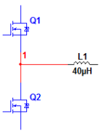
example.png
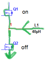
This shows the normal half bridge you find in every controller powerstage. A inductor is added as a reference to the motor.
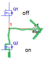
example1.png
In this example, current is flowing through the low fet (Q2) into the inductor.
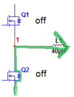
example2.png
Now the low fet is turned off. The inductor objects any change in current, so in this sketch you see the current take the path through the internal body diode of the low fet.
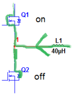
example3.png
This is a successfull switching: The turn on of the high fet allows some current to turn off the lower fets body diode. The turn on time is substantial enough such that the body diode have time to shut off. I make this possible by adding a series resistor to the bootstrap capacitor - slowing down the turn on, but not the turn off. This makes for a lazy switching, I use 400nS to turn the high fet on - else the low side fet spuriously 'malfunctions at around 200A, giving a dIF/dt = 500 A/μs. At 500 A/μs the reverse recovery time is about 350nS. Datasheet values is given at 100 A/μs and does climb somewhat exponentially.
example4.png
This is a unsuccessfull switching: The turn on of the high side fet is faster than the reverse recovery of the lower fet's body diode - this makes for an extremely low impedance between positive and negative rail, everything being absorbed by the mosfets. The literature is spread in what happens next, some show a kind of 'latch up - making for a permanent 'on' diode, and quite quickly fried mosfets. The other shows the diode shutting down 'as planned'.

There is a way to circumvene this problem: tune the high fet turn on directly after the turn off of the low fet. The body diode never conducts, and so there is no charge to be removed. Synchronous rectification at it's best. Dead time between fets is effectively zero between switches. I've made my own version in software, much alike TI's Predictive Gate Driver. My software works most of the time, but it pops a fet every now and then - considerable datalogging reveals the dead time being off shortly before the failure.

Therefore I'm looking for a way around this problem. I still want to tune a 'tight' dead time - but I wonder if some sort of turn off snubber may limit voltage rise time of the lower side switch. Since the snubber only needs to work one way, it can be made 'lossless' with a diode for decharging the snubber capacitor. I need feedback on this idea, has anyone done something like this? I'm at a loss trying to spec dV/dT or what this snubber needs to look like, any input would be greatly appreciated :D

I hope to have shed some light on mosfet useage in inverters, this switch instant - I'm sure - is often overlooked.

Ps: Note that the current direction in example 3 and 4 switches compared to the first examples - this is not the truth, a minor blunder :oops: The current will go the shown way, but not in an instant.
 
Looks interesting.
Do you have any data on how much increase power and efficiency you achieved with this method?
Seems like it may only be more power and not more efficient. I guess to the end user if you have a current limit and get to that (say 1kw) you may see a slight increase in torque?
 
Switching losses is nearly halved as there is no energy dissipated in body diode recovery. Efficiency gain, certainly yes. Reliabillity gain? Even more - EMI is greatly reduced.

As for power, power not lost is power delivered ;)

Again, can anyone shed some light on turn on snubbing (one way snubbing)?
 
I have had this problem in my mind since you poped up around with it (never had eared about it before).
Some say a schottky diode in parallel with the lower MOSFET will solve the problem, but others say the inductance of the schottky diode's path will not be able to prevent the MOSFET's diode from turning ON, given short switching times.
I ask, what if we make sure the inductance on the schottky's path is smaller, by not paralleling with the MOSFET "at the MOSFET" but having a path a little shorter (or making sure the path through the lower MOSFET has a little bit more inductance)? Always keeping the deadtime as short as possible with the predictive algorithm or such, to reduce the size of the needed schottky. I haven't played with this in simulation yet. Assuming it would work, what would be the advantage/disadvantage compared to a snubber? Questions questions questions...
 
I truly believe a well designed snubber is the way to go. Switch the lower fet on while the voltage is still low (whithout ever having the body diode conduct) and you should be good. The normal R (to bleed off the snubber cap), can be replaced by active switches for greater efficiency - but at added complexity.

This also has me thinking if snubbers makes my deadtime-algorithm useless. Since body diode conduction (I measure the characteristic voltage drop) is needed for feedback, my algorithm will not give any furter gain in performance compared to setting the deadtime fixed. I also believe the ease of proper snubbing is the reason Predictive Gate drive from TI never really catched on, it's worthless with snubbing.

Parasitic inductance can act as a kind of dI/dT snubber, i think. In my layouts the positive top drain and negative bottom source is as close as they can be - while the phase connections are longer and separate, to give some extra inductance so as to slow down possible shoot through.

Take all of this with a grain of salt, I'm up to my neck with this stuff and might have it all wrong. Need to sleep and think som more on it :p
 
IM trying to understand what you are saying your solution is Teh Stork are you saying when the low side is turned off you then turn on the hi side to save the low side diode?
If So I think this is what Lebowski is doing and Alan B has sugested to me a while back as well.
 
Arlo1 said:
IM trying to understand what you are saying your solution is Teh Stork are you saying when the low side is turned off you then turn on the hi side to save the low side diode?
If So I think this is what Lebowski is doing and Alan B has sugested to me a while back as well.

I believe you are somewhat correct on what Teh Stork is doing. When the low side is turned off, the inductance keeps the current flowing in the direction it was flowing when the mosfet was on, so the body diode conducts this current. In synchronous rectification, the high side fet is turned on after the low fet turns off so that the body diode never conducts. Right now Teh Stork measures voltage drop from body diode conduction in order to set his deadtime between low side turn off and high side turn on. However, I think he wants to use snubbing so that the body diode never conducts and the voltage spike from the motor's inductance is mostly absorbed by the snubbers until the high side turns on.
 
thepronghorn said:
Arlo1 said:
IM trying to understand what you are saying your solution is Teh Stork are you saying when the low side is turned off you then turn on the hi side to save the low side diode?
If So I think this is what Lebowski is doing and Alan B has sugested to me a while back as well.

I believe you are somewhat correct on what Teh Stork is doing. When the low side is turned off, the inductance keeps the current flowing in the direction it was flowing when the mosfet was on, so the body diode conducts this current. In synchronous rectification, the high side fet is turned on after the low fet turns off so that the body diode never conducts. Right now Teh Stork measures voltage drop from body diode conduction in order to set his deadtime between low side turn off and high side turn on. However, I think he wants to use snubbing so that the body diode never conducts and the voltage spike from the motor's inductance is mostly absorbed by the snubbers until the high side turns on.

Spot on, and I want to do it better than lossy RC snubbers.
 
Do you have the case below, Stork?

switchingseq.png
 
That looks right Njay, the diode affected is not in the FET opening up, it is in the opposite side of the half bridge. This way the decaying current forms a loop through the high side bus, the commutating high side FET that stays on and is off-schematic to the right, and the diode in the high side FET on the left.
 
Teh Stork said:
thepronghorn said:
Arlo1 said:
IM trying to understand what you are saying your solution is Teh Stork are you saying when the low side is turned off you then turn on the hi side to save the low side diode?
If So I think this is what Lebowski is doing and Alan B has sugested to me a while back as well.

I believe you are somewhat correct on what Teh Stork is doing. When the low side is turned off, the inductance keeps the current flowing in the direction it was flowing when the mosfet was on, so the body diode conducts this current. In synchronous rectification, the high side fet is turned on after the low fet turns off so that the body diode never conducts. Right now Teh Stork measures voltage drop from body diode conduction in order to set his deadtime between low side turn off and high side turn on. However, I think he wants to use snubbing so that the body diode never conducts and the voltage spike from the motor's inductance is mostly absorbed by the snubbers until the high side turns on.

Spot on, and I want to do it better than lossy RC snubbers.
There are more complex loss-less snubbers...
 
Njay said:
Do you have the case below, Stork?

switchingseq.png

I believe that you rarely see this in normal inverter operation. Especially sine, FOC or other controller algorithms that keep the current 90deg on voltage vector. In six-step, yes some - but not a lot.

Some reasons for that, as i see it - having trouble fully describing it, but here goes :)

- Current is normally 'sourced' from the low fet - not 'sinked'. Remember current flow is the opposite of the voltage applied.
- If you're trying to 'turn current in an inductor around' this needs some time. In normal inverter operation - I do not think this happens at all. Your sketch may show this, but then you shold continue to keep the low fet on, so not really.

Just as a reference:
00032.png
 
Per your last post, you seem to use the "real" current flow direction instead of the "conventional" direction (which I thought was the "standard" among EE). But this still doesn't make sense with your pics on the 1st post, because at some point (example 2) you set the current flowing in the same direction as the MOSFET's diode, but all symbols in electronics use the conventional current flow direction and not the real direction, so it should actually go through the top MOSFET's diode (as in my example) and not the bottom one. What am I missing here?

I have no brushless knowledge. The case I showed is the case you have in half-bridge or h-bridges to control brushed DC motors. In a half-bridge like the example, the current through the motor only flows in one direction (no regen assumed here). The thing with this case is, if you want to switching really fast, some say (never tested it myself, but makes sense) you will not prevent the diode from turning on with any external component, because the inductance between MOSFET and MOSFET's diode is so much smaller than between MOSFET and any other external component. Therefore, only something like TI's predictive algorithm would prevent the diode from turning ON. Again, assuming we want to switch the thing really fast; otherwise, the chinese controllers already solve the problem, by having really long turn ON times.
 
You're correct, this does not make sense. I've mixed electron and current flow at least one time here :|

Our EE physics book talks of electron flow, some of our other books talk of current flow. But yes, electron flow is against the pointy end of the diode symbol. And current flow the other way.

I'll have to go back to my journal to try to make some sense of all of this. I was pretty certain I was seeing the effects of what i described in the first post, but there is probably something like what you sketched Njay.
 
Njay said:
When going back from right to left, that is, when turning the top OFF and bottom ON, the top MOSFET diode will also turn on, but this time the reverse recovery current will go through the bottom MOSFET when it turns on.
I don't know if you see this case in a brushless controller (maybe if rotating the motor in reverse, which ebikes don't usually do), but the chinese controllers also turn the bottom MOSFET really slow... I guess this case could be snubbed.
 
For the inductance the voltage is

V = L * di/dt

When the lower left FET is conducting the current is rising in the inductor, and the V is opposing the applied voltage, so negative to the FET junction and positive to the off-screen commutation FET to the right that is conducting to the positive rail.

As soon as the lower left PWM FET opens the current will start to fall, and di/dt will change sign and V will change sign. So the left hand inductor terminal will go from negative to positive as the magnetic field collapses and generates EMF. This will take this terminal above the positive rail and the upper FET's body diode will conduct and clamp it to the upper rail plus the diode drop.
 
That's what makes sense, and also what I see. The motor wire will raise one diode voltage drop above the positive rail while the diode is conducting. You'll miss it easily on the scope if you're not expecting it, because it's a small variation (up to 1V or so) on top of the rail (usually >24V) which lasts only the deadtime (when doing synch rectification, which we really should do, at least when not regening).
 
Back
Top