converting meanwell power suply into Lipo charger

Hi Neil, glad someone else has got one :twisted:

I have emailed sure-electronics see if they offer me anything for sending the wrong model :(

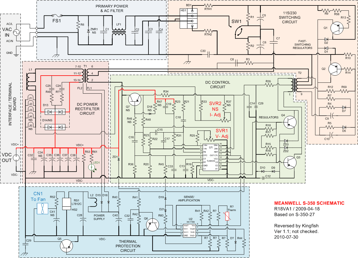
With this model having the constant current limiting circuit I am not sure if we will be ok using it at full power?

I am gonna put my batts on charge for a few mins and keep an eye on the current....

edit: just used mine to charge 4x6s lipos, current started at 9.5 and slowly went down to 1 or 2 amps after about 45 mins. the meanwell got a little hot but the fan soon cooled it down, no funny smells or explosions :) I think I am gonna keep on using it as it, I have seen in other posts ppl running them for months at this sort of current and no probs.
 
I see it has the standard looking shunt wires on the board, so one approach would be to simply snip one of them to get about 2/3 of the rated current. To make it adjustable, there will probably be a way, but I'd need a better pic of both sides to try and trace it out. There will probably be one of the op amp sections measuring the voltage across the shunt wires. Changing the gain of the amp will change the current limit.

The current sense line on the TL3845 is usually for the input side limiting, so not where you want to hack.
 
I found this on the data sheet for the TL3845

Screen shot 2011-09-03 at 19.16.37.png

I am wondering if Rs would be the shut, and there fore it is just a matter of finding Rf and adjusting that.

The board has a load of SMD's on the back and that makes it difficult to trace. Will try tracing the tracks back from the shunt to see if there is any similar link to pin 3 as per the data sheet
 
Nah, cant trace anything...just too tightly packed and with traces going under SMD's and then seemingly disappearing, it is not easy.

I have it charging now, as it is, at 49.8 volts on a 12s pack.

It has been drawing a constant 9 amps for a good 30 minutes now, and the fan only just starting to come on.

I used the supplied power cord...a weedy thing that I fear will catch fire it is getting so hot...but I will leave it for the moment to see what happens to it :twisted:


Edit ...update...well the power cord has not caught fire and the current output seems totally stable when compared to a S-350 when the fan kicks in and out.

On a S- series, when the fan comes on, the output current also increases. this does not happen with the NES model
 
shunt shave/clip/add solder will work, it's just like modifying a controller that isn't programmable..
Anyway that's unfortunate Neil.. that looks very different.. sounds like the community needs to get a-hacking again..
 
NeilP said:
I am wondering if Rs would be the shut, and there fore it is just a matter of finding Rf and adjusting that.

The board has a load of SMD's on the back and that makes it difficult to trace. Will try tracing the tracks back from the shunt to see if there is any similar link to pin 3 as per the data sheet

That's probably not where you want to look. The current signal from the shunt will be going into the (-) inputs of one of the error amplifiers, probably through one of the separte op amps first.
 
I will have another look, but from what I can see so far there is only one op amp IC on the board, and that is the HA17358B and that is the same IC as U2 on the S 350, in the lower blue shaded section, the thermal protection circuit

Meanwell_S-350-27-v1.1.png


http://www.hordsoffun.com/ebike/pics/Meanwell_S-350-27-v1.1.png

The only other 'control' IC is the one with the ISENSE pin. The other two 4 pin chips are opto couplers
 
In the schematic, you'll see the current signal from the shunt is going to the - input of one error amp.
On your new supply, there should be a trace going from the one side of the shunt, through some resistors, to the error amp input. It's possible they do it some other way, but I bet it's nearly identical.
 
Which one are you referring to ? U1 near SVR1 and SVR 2 or U2 in the blue shaded section?

On the new NES series..that first op=amp (U1 in the schematic above) does not exist. There is only U2 that is driving the thermal protection circuitry
 
U1 pin 15 is where R33 feeds in. You want to find the new "R33".
Looking at the datasheet for the TL3845, I'd guess the current limiter we want to mess with is going to the VFB pin (pin 2 on the 8DIP version). The voltage regulator is also going to feed into the same pin, so may be a lot of connections. Look for a trace that goes from that pin, through at least one resistor, to one side of the shunt wires.
 
OK, will do that tomorrow.
It is down in the workshop and I am ( or should still ) be in bed. It is now almost 5 in the morning...need to get some more sleep before work
 
Sleep is good.

If you can take a close up pic of the area around the chip, including the shunt wires, and the back side of the same area, it may make tracing easier. I did notice some pretty big blobs of white stuff covering some parts, so hopefully nothing important is hiding under there.
 
I've got a couple of power supplies- one a meanwell and another a clone. I was going to put a fechter current limiting board on but he's out of stock so then I thought I'd do the r33 mod.... but the clone doesn't have the current limiting circuit in it and the meanwell is an updated design with different board. It does have a scr1 transistor on it which may help?

Here's some photos of the boards- any suggestions as to whether I can get adjustable current limiting on either of these?


This is the new meanwell
bccef0d2.jpg


Just below the "NES" on the top of the board is the scr1 transistor
2b514abe.jpg


Back of the board...
182fb2a2.jpg


This is the clone (with variable pot installed at r33):
9c692e19.jpg


5ab44ccf.jpg


Rear of board:
566bd020.jpg
 
See Fechters advice to me earlier and then look. at the NES board, near the scr

See the 8 pin IC. U1, that is marked TL something
As Fechter suggests, see if you can trace pin 2 from that chip, via a resistor to the shunt

If you can find that resistor you may just have found the NES equivalent of the R33 resistor
 
Thanks Neil, I'll have a look tomorrow after work. Bedtime now down here! Some of us don't(can't) stay up till 5am...

Oh, and I know I'm going to look like a dummy here...but... which is pin 2? On the spec sheet I've had a look at, pin 2 is second from the left on the bottom row when the indent is on the left of the chip. This chip doesn't have the indent but a circular depression in the upper surface set off centre.
 
andynogo said:
This chip doesn't have the indent but a circular depression in the upper surface set off centre.
That's pin 1.
 
I was not staying up till 5am, more a case of waking up too early

I have the ssme supply, and will try and look myself when I next get a chance
 
I just had a look at your NES board. good pictures. i have cropped out a couple of smaller pictures that may be of interest.

First there is this line of Zener Diodes partially obscured by the transformer. on many of these supplies the OVP is driven by a zener driving pin#1 of one of the opto-isolators.
zener.jpgopto isolators.jpg

if the OVP voltage is high enough they may use a pair of zeners in series. you could trace back the pins of the opto's to see which one goes to one or both of the zeners. check the part # of that opto. if it is a SCR output type or if its output feeds the SCR device to the right of the opto's you have found your OVP circuit for sure. just add another zener in series to increase the OVP. They use an SCR because once it is triggered on it will not turn off until you turn off power to the supply.

The other opto will be part of the voltage regulator section. trace it back and you should find whatever circuit is used to regulate the voltage. maybe if you post some pictures of that someone could figure out where to attach one of Fechter's Mini-Meanwell Limiters.

rick

PS. I wonder what this OVP pad in this picture is used for?
voltage set pot.jpg
 
OVP is usually over voltage protection. This pad is generally where my limiter board would tie in and should have about 2.5v on it when the supply is running.

What is the marking on U100? It looks like the current limiting is going to be feeding through one of the optocouplers and not tied directly to U1.

It would be good to have a bit higher resolution picture of the area around U100 and the shunt wires on both sides.
 
I will have a look at my original pics tonight and see if i can crop out some more high res images...otherwise i am not back down the workshop till later tomorrow
 
See if you can get a closeup of the area circled in red. The black jumper wire is kind of in the way too.New Meanwell closeup area.jpg

See what U100 is.
 
I made mention of U100 earlier..though did not name it as U100...it is a HA17358B....... the same as U2 in the S-350 schematic I posted a link to earlier. Pretty sure I traced it out to the Thermal Protection circuit and thermistor ...same as in the S-350 series.

I did not take pictures of the back of the board, will have to see if andy has taken in closer ones and can get back with them before I do
 
Based on what I can see so far, I'd guess these resistors here are going to be like R33. Lowering the value should lower the current limit. I see one empty spot, wires could be attached and run to a pot.

I'd like to know what the value of the other two resistors is.New Meanwell closeup area2.jpg
 
What do you reckon is in that red circle ? would that be three resistors in parallel?

Just off down farm now to try and fit resistor to throttle line to give LVC Control from SA CA to ebikekit controller
If I have time I'll get closer pics of those areas
 
Looks like you may be correct. I assumed that because the IC U100 as the same device as in the S series menawell..then it performed the same function...well may be one half of it does, but the bank of 2 SMD resistors you circled earlier, connected to the positive side of the shunt, does connect to pin 6 on that U100 IC...which is a V- input on the error amp

Have reversed and overlayed the top to bottom of the board, in the images below, and left them full size but reduced the jpeg quality to allow uploading
 

Attachments

  • Circuit top reduced.jpg
    Circuit top reduced.jpg
    352.8 KB · Views: 3,256
  • Blended 3 reduced.jpg
    Blended 3 reduced.jpg
    349.6 KB · Views: 3,256
  • Blended 2 reducee.jpg
    Blended 2 reducee.jpg
    363.3 KB · Views: 3,256
  • Blended 1 redued.jpg
    Blended 1 redued.jpg
    385.4 KB · Views: 3,256
  • Circuit back reduced.jpg
    Circuit back reduced.jpg
    418.6 KB · Views: 3,256
Back
Top