Teslafly
10 mW
Progress update
Lots of stuff has happened since the last big update, and if that one was a "design" iteration, then this one is definitely a "test" iteration. This post is probably also longer than strictly needed, but I partially want to document this thing so I can go back and look back at it and see how it progressed, and partially for engineer eye candy.
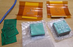
Boards arrived and I finally got my hands on them after sitting in the mailbox over break. One of each was promptly pasted and assembled as classes hadn't really picked up yet.
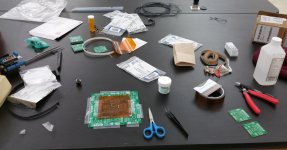
Assembling boards and definitely not hogging the entirety of 2 island tables.
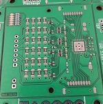
Tiny, tiny smd parts. Get a good tweezers.
View attachment 9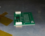
Reflowing in the toaster oven.
 View attachment 6
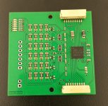
Hot off the presses.
At this point The only thing that was left was to test and refine the code. That only lasted all week...
For code changes I basically rewrote the burst receive function, which gets all the cell voltages and one temp adc reading in one swoop, but surprisingly everything else seemed to work almost off the bat.
View attachment 3
Testing mosfet outputs and ADCs. Everything works.
Once I confirmed that everything seemed to be working hardware wise, I made more.
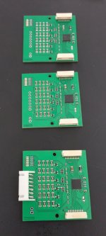
(so identical. much fun)
At this point the more sinister problems started to pop up. unreliability in adc reads, taking 3+ seconds to read instead of the advertised 8.2ms.
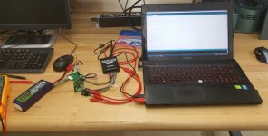
Logic analyzing the crap out of stuff. You gotta love practically living in an EE lab. (2 minute walk)
At this point I realized that the datasheet was lying to me, or at least leaving out some critical information.
Sure enough, after a thorough reading and a 500khz square wave from a signal generator, I confirmed that the CLK pin actually needed me to clock it, instead of what I had assumed would be a clock out in the absence of the datasheet specifying otherwise.
I was now reading things in the 8.2 ms advertised and getting reliable data every single time. The chip was working perfectly not that it no longer needed to relay on stray EMI to "ghost clock" the thing.
a few hours of coding later and a jaunt through the atmega328 datasheet and I configured timer 1 to toggle pin 9 at 500khz without using any computation time. a jumper was added and problem solved.
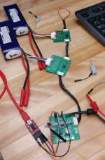
Everything working and looping through balance resistors to test them. Good data all around.
And in case a wall of pictures and text isn't your thing, have a video.
[youtube]nwdLbB5ceOw[/youtube]
The working code has been published to the github and the files are also included in the zip file below for easy reference.
https://github.com/Teslafly/OpenBMS
View attachment ATA6870N_Test_Program_2.0.zip
If you want more pics and such you can find full-size versions of most the pictures I took over here: https://www.flickr.com/photos/76027390@N05/sets/72157649986107399/
Up next: (This weekend?)
- Current goals
- Future plans
- Feedback
Lots of stuff has happened since the last big update, and if that one was a "design" iteration, then this one is definitely a "test" iteration. This post is probably also longer than strictly needed, but I partially want to document this thing so I can go back and look back at it and see how it progressed, and partially for engineer eye candy.

Boards arrived and I finally got my hands on them after sitting in the mailbox over break. One of each was promptly pasted and assembled as classes hadn't really picked up yet.

Assembling boards and definitely not hogging the entirety of 2 island tables.

Tiny, tiny smd parts. Get a good tweezers.
View attachment 9

Reflowing in the toaster oven.
 View attachment 6
Hot off the presses.
At this point The only thing that was left was to test and refine the code. That only lasted all week...
For code changes I basically rewrote the burst receive function, which gets all the cell voltages and one temp adc reading in one swoop, but surprisingly everything else seemed to work almost off the bat.
View attachment 3
Testing mosfet outputs and ADCs. Everything works.
Once I confirmed that everything seemed to be working hardware wise, I made more.

(so identical. much fun)
At this point the more sinister problems started to pop up. unreliability in adc reads, taking 3+ seconds to read instead of the advertised 8.2ms.

Logic analyzing the crap out of stuff. You gotta love practically living in an EE lab. (2 minute walk)
At this point I realized that the datasheet was lying to me, or at least leaving out some critical information.
Sure enough, after a thorough reading and a 500khz square wave from a signal generator, I confirmed that the CLK pin actually needed me to clock it, instead of what I had assumed would be a clock out in the absence of the datasheet specifying otherwise.
I was now reading things in the 8.2 ms advertised and getting reliable data every single time. The chip was working perfectly not that it no longer needed to relay on stray EMI to "ghost clock" the thing.
a few hours of coding later and a jaunt through the atmega328 datasheet and I configured timer 1 to toggle pin 9 at 500khz without using any computation time. a jumper was added and problem solved.

Everything working and looping through balance resistors to test them. Good data all around.
And in case a wall of pictures and text isn't your thing, have a video.
[youtube]nwdLbB5ceOw[/youtube]
The working code has been published to the github and the files are also included in the zip file below for easy reference.
https://github.com/Teslafly/OpenBMS
View attachment ATA6870N_Test_Program_2.0.zip
If you want more pics and such you can find full-size versions of most the pictures I took over here: https://www.flickr.com/photos/76027390@N05/sets/72157649986107399/
Up next: (This weekend?)
- Current goals
- Future plans
- Feedback


