MOSFET cooling in commercial controllers; how do they do it?

Thanks strantor.
After looking at previous posts about this type of beastie, excuse my niavity, did'nt realise they are'nt monolithic internally just multiple fet chips, understandable if manafacturer makes millions of 100A fets chips. Can see now why the professionals might want to parallel discretes
These modules might be good for additional cooling mods i've been obsessing about,if lid comes off them.
Can't understand massive heatsinks if a fet is going to be hammered for a few minute bursts, would think snap freezing might help, read somewhere fets take to freezing improves parameters massively where IGBT'S don't take to it.
 
megacycle said:
Thanks strantor.
After looking at previous posts about this type of beastie, excuse my niavity, did'nt realise they are'nt monolithic internally just multiple fet chips, understandable if manafacturer makes millions of 100A fets chips. Can see now why the professionals might want to parallel discretes
These modules might be good for additional cooling mods i've been obsessing about,if lid comes off them.
Can't understand massive heatsinks if a fet is going to be hammered for a few minute bursts, would think snap freezing might help, read somewhere fets take to freezing improves parameters massively where IGBT'S don't take to it.
Yes they are basically a bunch of FETs in one package. The difference is that when paralleling discretes, there are a lot more variables. different Ls, Cs, and Rs in the individual packages and in the circuit. in these modules they go straight to the source, bypass all the middlemen and parallel the devices at the silicon level which (should, we will see) eliminate all parallel-FET-induced problems currently being realized in the commercial controllers. Theoretically all the FETs in the module should always share the load equally. The only reason I can see for the big guys paralleling 30+ FETs on a board is to cut cost. For a guy like me making a one-off controller, I can't justify going through several revisions of circuit board until I stumble on one that fits (and probably end up spending more money in the end and definately more time) when this pre-packeaged solution exists.
 
Ok, I've been playing around with my module :D . came up a with a simple driver circuit:
View attachment 4

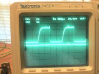
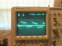
I'm using an arduino to generate the PWM (500Hz 5V 50% duty cycle) and creating a inverted copy of it to switch 2 darlington transistors to create a (should be) 5A 12V gate drive signal. It all seems to be working as planned...
View attachment 3

scope2.jpg

scope3.jpg

scope4.jpg

So as you can see, my circuit absolutely sucks at driving this MOSFET module. This is a 500Hz waveform. @ 20KHz I bet it wouldn't even turn on! What could be the problem? The whole circuit is on a breadboard and I'm using a 24awg jumper wire from the breadboard to the FET, and I'm not utilizing the "kelvin source" terminal. Would it perform better on a PCB placed directly on the gate terminal?
 
There are a number of things that may help:

  • The NTE534 is open collector design and is a little slow, about 3 or 4x what I would like to see. It's output impedance is too high with the open collector for fast switching.

    The totem pole needs about a 4.7uF or more tantalum bypassing it, not a 0.1uF

    There needs to be about 1 or 2 ohms in the gate of the BIG FETs to damp oscillations once you get them to switch fast.

    Basically the NET534 is not a FET driver. I like to roll my own totem pole (emitter follower) current amplifiers afer a IR2113S

    Zetex makes some great transistors for use in the emitter follower. We want speed and pulse robustness. I couldn't find switching characteristics on the TIP42, so you may have to measure it with your scope. The NTE2343 is a darlington! Slow, too slow...

    Your driver has DC current capability, but seems to be lacking in speed and pulse power capability. Basically not the parts I would spec for driving a brick.
 
strantor said:
Hi, thanks for that lengthy reply. I'm not yet schooled enough to address most of it; I am reading however, at a torturous rate. maybe in a couple of weeks I will be able to carry on a decent conversation on the topic. one thing I would like ask, regarding this:
Electroglide said:
Fets do share reasonably good if they share a common electrically connection point and share a common heat spreader. They are positive temperature coefficient devices...ie the Rdson goes up with temperature which means that parallel mosfets will reach an current equilibrium point that is dependent on the die temperature and the circuit impedance between the devices.
this seems to be disagreement with moose's last document he linked to (the way I interpret it). If you have a look in that doc, section III (b) (i):
For two
devices from the same date code, the predicted 18% maximum
unbalance is reduced to 14% allowing for temperature
compensation. For N large and without screening, temperature
compensation reduces the predicted maximum unbalance from
85% to 56%. Note that these reductions assume a common
ambient temperature. If a common heatsink is used, the
reductions will not be as large (refer to condition (b) above).
For simplified heatsink design, see reference 10.

and later on in section III (d) (vi)
Current unbalance due to ON resistance mismatch is reduced by allowing different junction temperatures. This reduction is
maximized for a large number of devices.
Seems to me, by using a common heat sink, you are "locking them in" to a common temperature, which undermines their intrinsic tendency to share the load.
I believe this paper was written in 1981, so things may have changed. Also, this paper seems very "theoretical", and I don't know whether to take the things is says literally, or if things in real life might be different. So, What say you? is it better to have separate heat sinks or common heat sink?

I have not been to this thread for a while, so I did not see the comments left behind. Reading quickly through the last document that you mentioned, the first thing that comes to mind is that the simulation was based on a circuit intended for RF which would be several orders higher in operating frequency than a standard motor controller. At those frequencies I would agree that mosfet sharing becomes somewhat more difficult since the time spent as a percentage of the duty cycle in the ohmic regions is longer and thresholds and device gains have a greater impact. Part of the simulation data at the beginning of the paper was given for mosfet on times of 900ns. That is shorter than most motor controller deadtimes. They also make some extreme assumptions like the gate resistors having 20% tolerance. I have never use anything other than 1% or maybe if I am desperate 5% tolerance resistors. 1% SMT 0603's are so cheap now a days why would you use a part with a large tolerance. Anyways I am digressing a bit. The gist of what I got from this paper does not conflict with what I had said previously though I may have not been clear about the sharing. When I said that mosfets in a parallel bank share well, I did not intend the statement to say they share perfectly equal current. The intent was to say that they share current in such a manner that you don't get the run away effects that you see when paralleling devices that are negative temperature coefficient like BJT's or the non-punch through IGBT's. In terms of a motor controller if one device it taking 500mA more current than it's neighbour, does that affect the big picture performance to any extent. I don't think it does. I think that when reading this paper, you need to take it as it is. It is a paper written on a series of simulations examining the effects of various parameters both within the device and external to the device separately. It does not study the combine effects that you would see in a real circuit and hence did not give much details on the interactions between all those parameters at the same time. So if I can summarize my thoughts on this paper, it says if you are operating at a lower frequency(like 20kHz) than the likelihood of having a "large" imbalance is low and there is less chance of going outside of the SOA for the device. The parasitic source inductance form the leads and the circuit path to the driver aids in the reduction of the dynamic imbalance due to feedback reducing the gate voltage to limit current. This is a well documented feature that supports the sharing of current within parallel mosfet banks that IR has had in their app notes for many years. The common heatsink does not aid in the sharing of current..In this case they are referring to all devices connected to a common heatsink without a thermal conductive electrically isolating interface. When I referred to a common heatsink I meant it to be used with a thermally conductive electrically isolating interface. (If you have noticed, not many people have controllers that don't use the tapes on their heatsinks) This is somewhat in effect the same as isolating the devices thermally which allows the individual devices to operate at slightly different temperatures, and yet still have the common heatsink temperature providing another temperature feedback mechanism. The tapes that I have used in the past are between 0.9C/W to 2C/W. So if a device is hogging more current the power dissipation will rise the die temperature slightly and increase the Rdson slightly thus reducing the current a bit through that branch. Layout really is everything when it comes to getting nice switching. Good symmetry helps too. I design back in Y2000 a 30kW 1000A 3ph traction controller that had 216 D2PAK mosfets on a IMS base. Each bank of fets had 36 mosfets in parallel. I did short circuit test that generated currents up to 2600Amps through these bases and never had a failure. I do know that every device did not have the exact same current, but it did not matter as long as they were not out that far I would be ok if they were out by 0.5A not that I could have ever measured it. On a side note, the high side mosfets did share a common heatsink because they were soldered to a common copper plate in that design. Still never saw any major issues with sharing that I could tell. I think that the biggest problem people have with designing pwm controllers is that they make the assumption that you just need to hook up the mosfets to a driver and you are done. In reality you need to size them for the power that you intend to run through them, you need to tune their turn on and turn off times to minimize the miller gate blips and Vds overshoots for both motoring and regen cases. you need to understand the thermal management of the design so that the devices don't overheat when running at rated power, etc, etc...lots to consider. Oh well...enough of my rants. This is why I like it here. If forces me to question my experience :lol: and it allows me to refine my knowledge.
 
There's something wrong with your schematics, I don't see how the TIP42 turns off, since it's a PNP and you're driving it with GND or 5V while it's emitter is at 12V. But let's assume the vcomp is powered by 12V and not 5V as in your schematics.

The osc figure shows that it's the charging of the gate that is slow. TIP42 datasheet shows typical gain of 50 @ 2A, that means it needs at least 2 / 50 = 40mA base current. The 2.2K base resistor only allows a max of ~5mA into the base.
 
Njay is right, I didn't even notice the voltages. If you want the short path to success. Drop in a IR 211x series FET driver, and then buffer it with what you learn on the attached app note. I also added the IR app note for buffering with FETs, it has some very, very nice demonstrated switching waveforms!

Good luck!
 

Attachments

  • ZetexTotemPoleDesign.pdf
    68.8 KB · Views: 74
  • HighCurrentFETbufferForDriver-dt92-2.pdf
    133 KB · Views: 79
Note I said the NTE2343 is a darlington. I did not say the TIP 42 was, I recognize a gain of 100 is not a darlington.
 
Sorry BigM, I was not referring to you, it was strantor that said it:

strantor said:
(...) and creating a inverted copy of it to switch 2 darlington transistors to create (...)
 
Whoops! :oops: Sorry, some "big guy" didn't get enough sleep last night... :oops: :oops:
 
I guess that explains the circuit's lousy performance, strantor thought he was dealing with 2 darlington and the resulting top drive ended up too weak.
 
bigmoose said:
There are a number of things that may help:

  • The NTE534 is open collector design and is a little slow, about 3 or 4x what I would like to see. It's output impedance is too high with the open collector for fast switching.

    The totem pole needs about a 4.7uF or more tantalum bypassing it, not a 0.1uF

    There needs to be about 1 or 2 ohms in the gate of the BIG FETs to damp oscillations once you get them to switch fast.

    Basically the NET534 is not a FET driver. I like to roll my own totem pole (emitter follower) current amplifiers afer a IR2113S

    Zetex makes some great transistors for use in the emitter follower. We want speed and pulse robustness. I couldn't find switching characteristics on the TIP42, so you may have to measure it with your scope. The NTE2343 is a darlington! Slow, too slow...

    Your driver has DC current capability, but seems to be lacking in speed and pulse power capability. Basically not the parts I would spec for driving a brick.
Great input, much appreciated!


Njay said:
There's something wrong with your schematics, I don't see how the TIP42 turns off, since it's a PNP and you're driving it with GND or 5V while it's emitter is at 12V. But let's assume the vcomp is powered by 12V and not 5V as in your schematics.
The osc figure shows that it's the charging of the gate that is slow. TIP42 datasheet shows typical gain of 50 @ 2A, that means it needs at least 2 / 50 = 40mA base current. The 2.2K base resistor only allows a max of ~5mA into the base.
Yes, it is probable that it never turns off. I have seen driver circuits that only use a NPN with a pullup resistor. my PNP is probably just acting as a pullup resistor if it is in fact not switching.

bigmoose said:
Njay is right, I didn't even notice the voltages. If you want the short path to success. Drop in a IR 211x series FET driver, and then buffer it with what you learn on the attached app note. I also added the IR app note for buffering with FETs, it has some very, very nice demonstrated switching waveforms!

Good luck!
Yes I am going to scrap this driver circuit and go with a real driver IC. I like the High current buffer circuit you linked to, thanks for that! While looking for driver ICs before, I ran across the FAN3122 (http://www.fairchildsemi.com/ds/FA/FAN3121C.pdf). It claims 7A peak output from the IC itself, with no buffer circuit. Also the IDX_630 (http://www.mouser.com/ProductDetail/Clare/IXDD630CI/?qs=sGAEpiMZZMvQcoNRkxSQkn6jLm8xbgsJXhV6HaofQC4= - For some reason the datasheet has disappeared since last week; I should have printed it while it was still available) which claims 30A output. Have you used a high output driver IC like this before? Would you think that it can match the performance of the buffer circuit?

Njay said:
I guess that explains the circuit's lousy performance, strantor thought he was dealing with 2 darlington and the resulting top drive ended up too weak.
DOH! Yes I did indeed erroneously think that the TIP42 was a darlington, hence the large gate resistor and minimal current.
 
Njay said:
You know, I was looking at the current source circuit with an ampop and thinking if we could get an ampop plus a transistorized power output to "force" a bunch of FETs to equally share current. We could loosely measure the current across the FET and compensate with temperature to avoid using the shunt. We could just then toss it FETs without matching, and I guess that would also forgive some layout "sloppiness". The reference for the ampops would be square wave with controlled raise and fall times, which would control the FETs to turn ON/OFF in a "synchronized" way. Could we make switch under 1us this way without expensive hardware and would it be worth it?

update: humm, it's an inductive load... not sure if the switching phase can be made without an external shunt. back to the books...
Njay I might be able to respond to this now. As far as measuring across the FETs (or, FET, in my case), I (currently, everything I say is subject to change) think this is a good idea, minus compensating for temperature. I think leaving the temperature as part of the equation gives us a better idea of actual power dissipation, which is more meaningful than current alone. It will however require a circuit to disable the current sensing while the FETs are OFF, since full pack voltage will be across the "FET acting as shunt" at that time. And not just when it is OFF, but after it is fully ON, as the opamp will read the turn-on as a very high current and shut it off again. you mention a square wave reference, but I don't think that's enough; I think it needs the input actually disabled during off-time.

I want to wait and see what the resistance of my bus bar is. I'm thinking might just use the bus bar itself as a shunt resistor, but I really have no idea what resistance value to expect from a bus bar. it will probably turn out to be way way too low resistance to use as a shunt.
 
Couple things as I look more. I must have been dsylexic on looking at your NPN PNP stack. I use an emitter follower as in the data sheets (NPN on top, PNP to GND, bases connected), your topology is different... I should have commented on that before.

The FAN3122 is a low side driver only. Since most of what I do is bridges, I stick with half bridge drivers.

The data sheet you are looking for on the IXDD630CI is here: http://www.clare.com/home/pdfs.nsf/0/6AC7CC624179BDA185257873005D6BE4/$file/IXD_630.pdf It is a low side part. Same limitations as above.

I think I posted this before, but if it got lost in the mush, here is my FET driver short list. I have standardized on the IR2113S for performance/cost trades. I do the tailoring in a roll your own buffer. There are parameters there I like to tune to get rid of ringing, and to do my stuff I need independent access to the emitters. The really high current drivers are typically low side only. When you add the price of a half bridge and two high current drivers, it is cheaper to roll your own, plus you get to tailor "things." I use the Zetex ZXGD3004E6 in the mid size stuff.

If you are experimenting, and wanting to build your knowledge and capability towards driving a brick. The IR data sheet I posted is pretty good with the FET buffer. You can get some good compact NFET/PFET in a SO8 pretty cheap. Take a look at the Alpha & Omega AO4612 as you move into driving the bigger stuff.

I like incremental development. NOTHING goes right the first time, and not all of it the second. By the third roll of the board most things work. Turns 4 to 6 perfect things; and then it is time to try something new. That means if you were apprenticing in my lab, I would have you build a IR211x driver for a single TO220/TO247, make it work and observe scope traces. Now parallel 3 TO220's with the same load. What do you see? What needs to change in the driver circuit? Now parallel 6 TO220's with the same load. What do you see? What needs to change? Now drive your brick, with the light load. What do you see? What needs to change? This process lets you learn more, and understand why you are doing what you are doing... it costs less in smoked/catastrophic events also! :wink:
 

Attachments

  • FETdriving-V1.pdf
    35.4 KB · Views: 74
Ok, I am going to play around with the IRS2113S, PFET/NFET buffers, and PNP/NPN emitter follower totem poles and also some of the high current drivers next week when I get paid. Until then I will be working on my control circuit. So far all I have is a set of ideas, largely influenced by your previous suggestions and those of others in my threads and other threads, with some of my own ideas:

fixed 20KHz 99% duty cycle PWM from a 555 or some other PWM generator
.001ohm sense resistor (or other) - 500mV @ 500A (250W @ full power, may need a lower value)
0-5V analog reference voltage from microcontroller (DAC) corresponding to throttle position (et.al. *)
An opamp will turn the 0-500mV (0-500A) signal from from the sense resistor into a 0-5V (0-500A) current feedback signal
A Comparator will compare the microcontroller analog reference to the current feedback signal
If at any time the current feedback signal becomes greater than the microcontroller analog reference, the PWM will be terminated for the remainder of the period (latch off, to prevent multiple turn-on attempts within the same period, accomplished by the shutdown pin of the IR2113S ot the enable pin of other ICs)
At the beginning of the next period the latch and process will reset

*there will be a hall current sensor on the controller output which will monitor average current
There will be a thermister in the motor and one on the controller heat sink
the microcontroller will monitor the average current and the 2 thermisters.
If the controller or the motor gets too hot, or if the motor draws too much current for too long, the 0-5V output will be reduced.
This will allow high current bursts (above rated motor current) during acceleration and allow the motor to realize it's 300A for 1min rating without having the driver monitor a stopwatch

If the MOSFET itself is to be used as the "current sense resistor" (I'm currently not planning to do this) then an additional circuit will be needed:
the mV output of the "MOSFET acting as a sense resistor" will become a 96V output when the MOSFET is OFF, so there will need to be some sort of switch to open the signal at any time when the MOSFET is not fully ON
This will require a set delay to allow full turn-on to occur, and the signal will need to be opened before turn-off begins to prevent signal voltage spike. I have no idea how to do this as I suspect it would require "seeing into the future"

Any input?
I'm currently trying to put these ideas into circuit form in LTSpice, but having trouble. learning to use LTSpice as I go. I will post up what I got once I have something.

Thank you for taking the time to help me out.
 
Stantor you have a nice start at a true phase current limited topology. Now you have discovered one of the reasons I like the IR2113 the shutdown pin. Put a current sensor in the phase lead, take an absolute value of that sense current around the 0 current value (rectify it relative to "virtual" ground) then use that to feed an SR latch that pulls the IR2113 shutdown pin. Reset the SR latch with your 555 timer circuit.

Nice job!
 
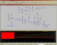
Ok so here's my convaluted current limiting scheme. What I did seems(?) to be doing what it is supposed to. What it is supposed to do, is look at an analog voltage (0-5V) coming from my microcontroller and limit the current based on that. 1V corresponds to 100A, and so on. I have set it to .5V for a 50A limit. As the current climbs and reaches it's limit (50A) in the 99% duty cycle, the MOSFET is shut off for the remainer of the period. At the beginning of the next period, the latch is reset (by the inverse of the 99% duty cycle, a "one-shot" so to speak) and if the current is <50A, the MOSFET is allowed to turn on, unit 50A is reached, at which time the MOSFET is shut off for the remainder of the period, and so on. So, from the simulation I can see that once 50A is reached, something happens, but not what I expected to happen. After the MOSFET turns on the current continues to climb but there are brief moments where it drops down to 50A. I think what is happening is that the MOSFET is too slow to turn off, allowing current to still pass. Do you know of a clever way to make this work?
RED = gate drive voltage
GREEN = current through Sense resistor
BLUE = mV output of sense resistor
motorcontrolcircuitsim.JPG

I tried to attach the LTSpice file but it doesn't seem to be working. I can send to anybody if they want to play around with it.

edit: BTW the component part #s listed are just dummy part #. circuit is for proof of concept. I really have no idea what actual components I will use.
 
When current limiting kicks-in, it seems you are just disconnecting the complementary pair's input. This is not "active turn off", I believe the transistors will still be a little bit of time ON, because of parasitic capacitance and this "charge removal" thing. You need to pull the input to GND.
 
Stantor, I am a bit rushed today. Yes your gate is slow, it needs to traverse in 500nS to 1uS max. Next low pass filter your sense resistor output. You need to deglitch it with the LP filter.
 
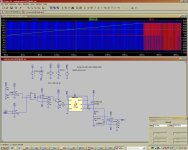
I was able to get current limiting working by changing to high side switching so I can monitor the current not only through the motor but the diode as well.
motorcontrolcircuitsim2.JPG

EDIT:
blue= gate drive signal
Green = current through the motor
Red = current through the diode

By using a high side switching, I would also get a little experience for my future brushless build. what say you?

I probably still need to filter the signal though
 
strantor, I think you would be better trying to understand why a circuit doesn't work (and fix it) instead of jumping right away into something totally different. What have you learned from your previous circuit, besides that "it doesn't work"?...
 
Back
Top