jonescg
100 MW
Hi everyone,
Been a long time since I started a new thread in this part of the forum, and it's not entirely battery related. But I'm wondering what some folks use to make PCBs.
I've had some success with geda PCB: http://pcb.geda-project.org/
The program is quite simple, but I'm not using it to it's full potential. I'm only ever doing two sided boards (components on top, solder through holes on the bottom). I haven't even worked out how to use the footprint features. Still, it's allowed me to make some battery PCBs which I have been using for my High Powered Lipo packs.
Unfortunately, the results are a bit hit-and-miss. When I export a PCB in gerber format, I then zip these into a folder and send it to a fabricator, usually in China. I'm finding OurPCB to be pretty good.
However sometimes the results are weird, like this one -
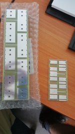
The drill layer includes a series of slots which are 1 mm wide and about 14 mm long. This is where the cell tabs go. It's almost as if the drill layer wasn't included in the export or something...
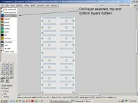
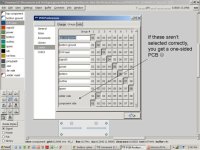
In "Preferences" I can select the Layers tab and allocate the features I want. I've been caught out here before, but the drill layer has never been an issue:
When I'm done I export them as gerbers, and it creates a list of files like so:
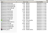
Now I presume the .cnc file is the one with the slots detailed. Also, the .pcb file even has details of the drill layer:
So how come I got a delivery worth $800 of PCBs I can't use for anything? Did they cock up or did I? Both are equally possible.
Been a long time since I started a new thread in this part of the forum, and it's not entirely battery related. But I'm wondering what some folks use to make PCBs.
I've had some success with geda PCB: http://pcb.geda-project.org/
The program is quite simple, but I'm not using it to it's full potential. I'm only ever doing two sided boards (components on top, solder through holes on the bottom). I haven't even worked out how to use the footprint features. Still, it's allowed me to make some battery PCBs which I have been using for my High Powered Lipo packs.
Unfortunately, the results are a bit hit-and-miss. When I export a PCB in gerber format, I then zip these into a folder and send it to a fabricator, usually in China. I'm finding OurPCB to be pretty good.
However sometimes the results are weird, like this one -

The drill layer includes a series of slots which are 1 mm wide and about 14 mm long. This is where the cell tabs go. It's almost as if the drill layer wasn't included in the export or something...

In "Preferences" I can select the Layers tab and allocate the features I want. I've been caught out here before, but the drill layer has never been an issue:

When I'm done I export them as gerbers, and it creates a list of files like so:

Now I presume the .cnc file is the one with the slots detailed. Also, the .pcb file even has details of the drill layer:
So how come I got a delivery worth $800 of PCBs I can't use for anything? Did they cock up or did I? Both are equally possible.

