power stage musings

Lebowski

10 MW
Joined
Jun 27, 2011
Messages
3,412
Location
beautiful Zurich, Switzerland
I'm starting this thread because of my suggested gate-drain RC network in Arlo's output stage thread. It seems to work well
in Arlo's 15kW controller so I wanted to investigate this technology myself. First measurements showed something
different from what i expected, so all the more reasons for an in-depth look. I'll probably update this first post of the thread
as I go along, not to have information lost and impossible to find somewhere in the middle of the thread.

Plus the weather here is crap so nothing better to do :?
DSC01227.jpg

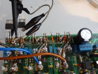
This is the output stage at the start:
DSC01229.jpg
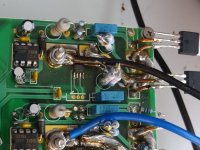
Two 4115's driven by a IRS2186 gate driver IC. The snubber components are disconnected. As a supply I'm using a 60V 2.5A
lab supply. I will only look at one output stage and use the PWM test function of my controller IC as the signal source.

The load is a big inductor and a few power resistors:
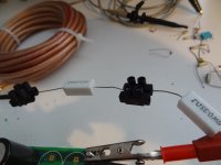
DSC01228.jpg

Because I don't really like the 'just add more capacitors' approach I use only two capacitors on the supply rail:
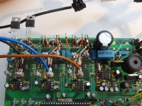
DSC01230.jpg
The caps are on the right, the big black cilinder is a 220uF cap with probably quite a high series inductor, underneath
it (the blue block) is a 470nF low inductance capacitor.

DSC01231.jpg
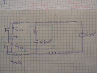
This is the schematic of what we have. On the right is the power supplies, which is connected with two long wires to the PCB. The long wires
represent quite some inductance. The 470nF capacitor is added to short out this inductance so the power stage doesn't see it, but it's not
100% succesfull at doing this as it has a small internal inductance itself. Going left from the 470nF we get the inductance of the PCB traces and
then the two 4115's.

The difficulty is now that when the output to the motor switched from rail-to-rail, the PCB inductors together with the output capacitor C_oss (of the
switched off transistor) causes ringing which overvolts the transistors and blows them up. Two strategies exist to prevent this. So far I've always used
the drain-source snubber approach, where an RC series network is placed across the drain-source of the transistors. The values of the RC are
chosen such that the ringing is greatly dampened. So, kinda the 'switch hard, ringing will be there but lets deal with it' approach.

The other approach, which is the subject of this thread, is the 'switch gently so no ringing will occur'. More technical, switching hard puts a whole
spectrum of frequencies on the output, the LC filter of the supply/C_oss selects the one it likes and amplifies it. Switching softly means the LC_preferred
frequency is greatly reduced in the output, so that there's not a lot going on at the LC frequency and hardly anything present to ring with.


First order of business is to see which transistor determines what. We have rising and falling edges in the output signal, and the transistor
in control depends on the direction of the motor current.
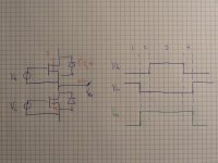
DSC01232.jpg
The picture shows the two output stage transistors, the high side being controlled by driver voltage V_h, the low side transistor controlled by V_l.
On the right you see the no-overlapping waveforms (with the deadtime) of V_h and V_l. There are 4 phases the output stage goes through during
one cycle of the PWM frequency, marked 1 to 4. The output to the motor is marked V_m. In this first picture the motor current I_m flows into the
controller as marked by the arrow.
During phase 1 with V_l high, the low side is on and carrying all the motor current. When the low side switches off I_m has to keep flowing (because
of the motor inductance, which acts as a current source), the only path open to it is via the high side diode (phase 2). When going from phase 1 to
phase 2 the motor voltage goes from low to high, as the motor terminal is kind off shorted to the high supply via the diode in the high side transistor.
The slope on V_m when going from phase 1 to 2 is controlled by the switching off of the low side transistor, so it is controlled by whatever gate resistor
etc we have in the low side.
Going into phase 3, the current is transferred from the high side diode to the high side FET. At the motor terminal you don't really see this as it
stays connected to the high supply. This means that the high side FET can switch slow or super fast, we just don't see it, the motor terminal
stays at the high voltage.
Goind to phase 4, the high side FET is switched off and the current is transferred to the high side diode. Again, this is not visible at the motor terminal
so, whether the high side switches slow or fast, we don't see it.
Going from 4 to 1, the current is transferred to the low side FET, the motor terminal voltage V_m goes low. The slope of V_m depends on how fast
or slow the low side switches.

The situation changes when the direction of the motor current is reversed.
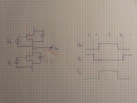
DSC01233.jpg
The reasoning is the same as the previous picture, except this time all the transitions of V_m are controlled by the high side transistor.

So, to summarize, with current going into the motor the rising/falling edges of V_m (and all the ringing) are determined by the high side FET, with
current coming from the motor flowing into the controller thre rising/falling edges of V_m are determined by the low side FET. It is important to
realise it is not as straightforward as saying the high side FET determines the rising edges iof V_m and the low side FET the falling edges !

As an intermezzo, notice how the effective width of the V_m signal depends on the motor current, dependent on I_m's direction V_m is wider
or narrower by an amount of twice the deadtime. Notice also that it opposes I_m, when delivering I_m to the motor V_m is narrow (so in
effect represents a lower voltage). This is as if there is a 'virtual resistor' in the system. A larger deadtime represents a larger resistor... not good.
 
Lets get some measurements to have a look what happens when we switch the output stage. It will be interesting to see the voltages
across the FETs for both hig/low transitions and for both current directions. To be able to judge the voltages across the FETs we should measure
both the output to the motor and the supply voltage at the FETs, both with respect to the ground at the FETs.
DSC01242.jpg
The output to the motor voltage shows whats happening across the low side FET, the supply minus the motor voltage shows whats
happening at the high side FET.
First the case of the current flowing from the controller to the motor. The load inductor/resistance is connected between output and ground.
View attachment 5
To generate a current we get the controller IC to generate PWM test signal with a specific deadtime and dutycycle.
Code:
a) PWM frequency: 21kHz
b) deadtime: 999ns
c) dutycycle testsignal: 5%
d) toggle high side polarity, now active HIGH
e) toggle low side polarity, now active HIGH
f) test PWM signals
z) return to main menu
The dutycycle is chosen at about 5%. With 65V supply this generates an effective (or average) voltage of about 3.25V across the load. With
about 0.7 Ohm resistance this should give about 4A flowing out of the H-bridge. The deadtime is chosen long just to not interfere with the measurement.
DSC01237.jpg
View attachment 3
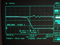
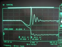
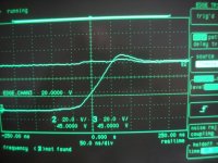
Both these transitions are controlled by the high side transistor. The falling transition looks kinda nice, has a not too steep slope to it and generates some
ringing in the supply but not too bad. The ringing here is across the high side transistor.
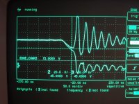
The rising transition for some reason (will explain why later) is super fast and sets off a huge amount of ringing in both the supply and the motor output
voltage (that both ring is not strange considering that the high side is on and effectively shorts supply and output together). The ringing is mostly across the
low side transistor. And it's a lot, 20V/devision you can see the peak of the ringing exceeds 120V, even though we only use a 65V supply. A 4110 would
have been fried already...

The other case is for the current flowing into the controller.
DSC01240.jpg
The load is now connected between the supply and the H-bridge output. To generate the same current as in the previous case, this time we need a 95% dutycycle.
DSC01235.jpg
DSC01234.jpg
Because of the current direction, this time both transitions are controlled by the low side transistor,
Now the falling transition looks horrible, with up to 140V peak across the high side transistor. The rising transition looks nice and controlled, with
only a small amount of ringing (across the low side transistor)
 
Before looking at whats happening during the switching events, first some basic theory about whats going on. I'm using the 4115, so here's the datasheet:
View attachment irfb4115pbf.pdf
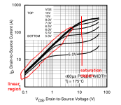
Most of the time the transistors are either off or on. In the on-state the transistor is in what is called the 'linear region', it can be modelled as a resistor (this
is well know here on ES). During the (short) transitions between on-off the FETs are in what's call the 'saturation region'. The transistor is in this
region when its conducting current, but the voltage across the drain-source is more than just a few V. So for instance, when it's busy switching on and it
carries like 20A of current but the drain-source voltage is still 30V or so, this is when the FET is clearly in the 'saturation region'.
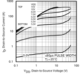
curves.png
In the above graph you can see, in the linear region the current depends on the drain-source voltage, so the FET acts like a resistor. In the saturation region
the current is (by approximation) not dependent on the drain-source voltage, only on the gate-source voltage. Here the FET is acting as a voltage controlled
current source. A voltage controlled current source (VCCS) is said to have a certain transconductance, which is delta_I / delta_Vgs. At the
red line for instance, going from 5.5 to 6.5V for Vgs the current goes from 50A to 150A, so the transconductance is 100A/V. This number can also be
found in the spec of the transistor:
View attachment 6
With the VCCS model of the transistor we can drawn what's in the industry called a 'small signal equivalent' schematic.
DSC01243.jpg
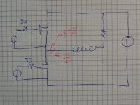
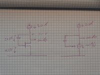
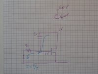
On the left is the schematic I want to discuss. We have a FET being fed with a 20A current source. A 4115 needs about 5V Vgs in order
to cunduct this amount of current. The output is, lets say, 30V, so there's 25V on the capacitor which I placed between gate and
drain. This is a stable situation, the gate-drain capacitor is ot charged or discharged so stays at 25V.
On the right is the small signal equivalent. As discussed, the transistor is replaced with the VCCS, with a transconductance of 100A/V.
The gate-drain capacitor is connected between the output and the controlling node of the VCCS.
Now, let see what happens if some outside 'force' tries to put a voltage on the output. Lets say it wants to increase the output by 0.5V.
Because the charge on the capacitor does not change, the 0.5V increase at the output also becomes a 0.5V increase at the controlling
node of the VCCS. The VCCS will respond by drawing 50A (100A/V * 0.5V) extra current, in effect pulling down the output node
against the will of the 'outside force' . This opposition from the VCCS in effect means the output impedance of this little circuit is very low
(it is in fact 1 / 100A/V = 0.01 V/A or 0.01 Ohm).
So, what the FET circuit does is that the voltage on the capacitor is placed at the output and has the full 'force' of the FET behind it.
A second thing that happens is that the 5V on the gate remains constant for a large range of the output voltage. If you look at the F shaped
curve above, 20A through the transistor means the gate-source voltage is around 5 to 5.5 V for a drain-source between 50V and less than
1V. So, for all intents and purposes, the drain-source voltage has no influence and the gate-source voltage is constant.

Lets add a resistor and a switch and see what happens.
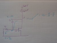
DSC01244.jpg
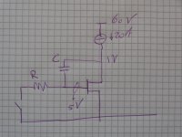
A resistor is added between the gate and an (open) switch to ground. The drain voltage is 1 V,because of the feedback action and the 20A current
the gate voltage is 5 V, and there's -4V across the capacitor. As long as the switch is open this is a stable situation and nothing will change. Now
lets close the switch.
DSC01247.jpg
The switch is closed and a current starts to flow through the resistor. Because of the feedback action the gate voltage will remain at 5V, so the
current through the resistor is 5/R . This current has only one way to go, through the gate-drain capacitor. The capacitor will be charge with the
5/R current coming from the resistor.
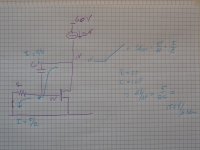
DSC01249.jpg
The voltage on the capacitor (and hence the circuits output) will increase with a slope delta_V/delta_t = I / C . Since the 5V on the gate is constant,
the current is constant so we have a constant, straight slope at the output of the circuit.
DSC01250.jpg
The slope can be calculated as shown in the picture above. With a 33 Ohm resistor and a 1nF capacitor the slope is about 150V/u-sec.
All the time during the slope the feedback action is active and the output voltage has the full weight of the FET behind it. So the slope
at the output has a 0.01 Ohm output impedance, it's not budging for anything or anyone.

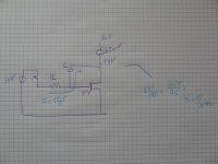
DSC01251.jpg
The picture above shows the case for a slope downwards. The output in the example starts at 59V. Instead of to ground the resistor is
switched to a 15V voltage source. Current will flow and with the component values as they are we get a 300V/u-sec downward slope.
 
With the theory in mind, lets have a look at the easiest case which is the low side switching off with the current flowing into the
controller. This is basically the case discussed in the previous posts.
DSC01252.jpg
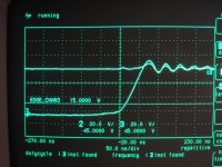
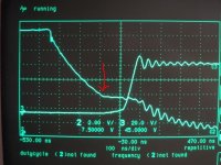
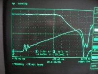
The screenshot above shows the output or drain (marked c3 on the right) and the gate (which is the green trace :mrgreen: c2) both
with respect to the source (ground as this is the low side transistor).

Going from left to right we see first the output is low and the gate is at around 14V. After about 150 nsec the driver chip switches to
ground. The internal gate-source and gate-drain capacitors of the 4115 start to discharge and the voltage on the gate drops While this
is happening the transistor still is in the linear region, it's acting as a resistor but it's resistance is slowly increasing. 250nsec
later we arrive at the point indicated by the red arrow. This is where we get into the saturation region of the transistor and the whole
theory of the previous post comes into effect. The gate voltage stops it downward slope and stays constant at around 5V while the drain
voltage starts to rise. Funnely enough though the drain voltage doesn't rise in a linear fashion but first has a gently slope (till the drain
voltage is about 7 V) followed by a steep slope. Once the drian reaches the 65V supply the saturation region ends and the transistor
is off. There is no more feedback action, the gate voltage continues it's downward slope till it reaches ground.

Now, the hockeystick curve at the drain while in saturation comes as a bit of a surprise. Again the datasheet of the 4115 provides the
answer. The capacitor between gate and drain (from the previous post) is a parasitic capacitor which is inside the transistor. The
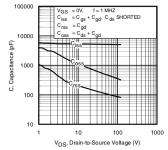
datasheet provides the following information regarding this capacitor:
c_gd.png
The legenda says that the C_gd is called C_rss in the graph. It is heavely dependent on the drain-source voltage of the transistor, it
starts out very high (1 nF) and it's value drops quickly as the drain-source voltage rises (0.3 nF at 5V, 0.1 nF at 60V).
So, when the gate drops down and arrives at 5V, the drain-source voltage is still 0. The C_gd is very large, 1nF, so the slope at
which the drain-source voltage rises is very gentle. But with an increase in drain-source voltage the C_gd value drops, the slope will
get steeper and steeper. The result is the hockey-stick curve we see in the measured output voltage.

Interesting is to calculate how much charge was supplied into the C_gd during the hockeystick transition. Looking at the graph, this
phase lasts for about 160 nsec (from the red arrow to the output reaching 65 V). During this time the gate stays at around 5V, so
with a 33 Ohm resistor a constant 150mA is drawn from C_gd. 150mA * 160 nsec gives a total charge of 24nC.

The spec gives a Q_gd (gate-drain 'Miller' charge) of 26nC which fits nicely with our 24nC....
 
For the investigation of what happens during the other (much more violent) switching event it would be nice to have an idea of the circuit inductance.
DSC01231.jpg
It would be nice to know the total effective inductance to the right of where the FETs are, so of all the wiring and in combination with the internal inductance
of the 470nF capacitor. The inductance can be calculated by looking at the ringing frequency. When for instance the current is flowing into the H-bridge and
the low side switches on, the output capacitor C_ds of the high side transistor (or C_oss in the picture above) sees a big voltage step which sets of the ringing.
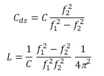
The ringing frequency is then given by the combination of C_ds and the inductance external to the transistor. The equation is

View attachment 3

Now, since the C_ds is not really know (it's a graph in the datasheet as shown earlier, very non linear) I want to do 2 measurments. One with just C_ds, and one where
an extra capacitor of known value is placed in parallel to C_ds. So:

measurement 1, only C_ds, gives ringing frequency f1
measurement 2, C_ds with in parallel known capacitor C, gives ringing frequency f2.

With these 2 measurements C_ds and L can be calculated

eq.jpg

In my case, f1 was measured at 27.2 MHz. Then with an extra C of 4.7 nF the new frequency f2 was measured at 7.7 MHz.

This results in:

C_ds = 410 pF
L = 84 nH

The L is the total inductance external to the transistors, so 2 times the trace inductance of the power lines plus the inductance inside the 470nF capacitor.

To verify, the online inductance calculator at
http://www.technick.net/public/code/cp_dpage.php?aiocp_dp=util_inductance_calculator
results in about 62 nH for the PCB traces alone, so the 84 nH looks reasonable.


The second thing that is important in the more violent switching event is the Reverse Recovery of the FET diodes.
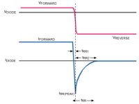
What reverse recovery comes down to is that when the voltage across a current-carrying diode reverses, it takes
a little bit of time for the diode to switch off. Before it switches off it will keep conducting ! This little bit
of time is in the order of 50 to 100 nsec. In a graph it looks like this:
reverse_rec.jpg
As you can see, even though the voltage has reversed and the diode should be off, current still flows during time t_rr.
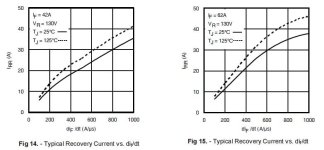
The data sheet unfortunately only has limited graphs for this, ahem, 'feature'.
irr.jpg
When the voltage across the diodes is reversed the current through them drops from I_forward to I_RR at a certain
speed (given in A/usec). The above graphs show I_RR as a function of this speed but unfortunately only for 2 values
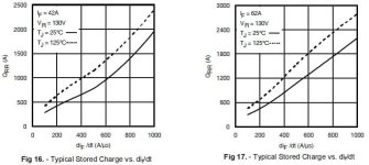
of I_forward. A second set of graphs shows how much charge manages to flow before the diode switches off.
qrr.jpg
This can give you an idea of the power loss due to reverse recovery. Charge Q = I * t, so V * Q = V * I * t. So supply voltage
times charge gives you joules . So lets say Q_RR is 2000nC, with 65V and 21kH PWM this is a loss of 2.7 W...
 
After the brief intermezzo with the inductor measurement and the Reverse Recovery behavior of the diode, back to the business at hand. We're
looking at the case where the current is flowing into the controller:
View attachment 10
Switching on the low side FET (phase 1) comes just after the current has done a dance from high side diode to FET back to diode. Lets see
how the motor current flows when we go from phase 4 to phase 1:
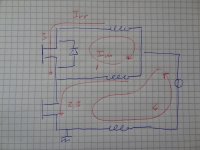
DSC01266.jpg
During phase 4 the motor current I_m is running around in a circle through the high side diode (indicated by the 1). As the low side transistor
switched on more and more of I_m is flowing through the low side, until all of I_m is flowing through the low side FET (indicated by the 2). Then the
nasty happens, the diode in the high side keeps conducting until a current I_rr flows through both the high and low side (indicated by the 3). Finally the
diode shuts down and all of I_m is running in the circle marked '4'.

The interesting thing is that during the current transfer the current in the positive supply parasitic inductance changes from -I_m to +I_rr,
so over a range I_m+I_rr. The current in the negative supply parasitic inductance changes from 0 to I_m+I_rr. So, both inductors show the
same current step meaning we can treat them as a combined inductance (we don't need to look at them separately).
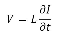
Because the current through the inductors is in a real hurry when it makes the I_m + I_rr transition, we can expect to see a voltage in accordance with:
L_drop.jpg
Just to instill the seriousness of this: with 84nH, a delta_I of 10A in a delta_t of 50 nsec, this gives a drop across the wiring of 17V :shock: .... just so we know
what to expect :?

DSC01257.jpg
the above picture shows both the supply and the output during the switchin event. The top trace is the supply, you can see how the I_m+I_rr change in current
causes a 20V drop across the 84nH supply inductance. The bottom trace (the output) stay pretty close to the supply, at first because the current in the high
side diode needs to drop from I_m to 0 and then secondly because of the reverse recovery effect. But once I_rr has been reached the diode stops conducting
and the traces separate, the supply bounces back to 65V and the output drops to ground.
DSC01258.jpg
This picture shows the supply and the gate signal of the low side FET. When the gate driver switches to a high voltage, because of the gate resistor
the signal on the gate rises with a ramp. There's no current through the FET in the beginning because the gate signal has to reach the FETs threshold
voltage (V_t). At around 5 V the FET start conducting, and judging by the (almost linear) drop in the supply voltage it's pulling a lot of current in a hurry.
DSC01267.jpg
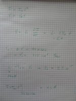
Above shows an approximate calculation of the current, assuming the voltage across the supply drops linearly with time. The calculation shows a peak
of 5.3 A (I_m+I_rr), while the motor current about 2.5A (I_m).
DSC01259.jpg
This picture shows the gate signal together with the output voltage. There's something funny going on here. According to the picture the gate voltage
on the FET is about 7.5V and there's 40V across the FET. It should be conducting way more current than just 5.something Amps.
current.png
This picture (datasheet) shows it should pull more than 100A. The only reason I can think off the FET is drawing a lot less current is that the source
voltage is higher than we think... If the gate voltage is measured correctly then the source voltage at the silicon inside the FET housing is higher
than we measure outside, which also means we should see a voltage drop across just the source leg of the FET itself.
View attachment 2
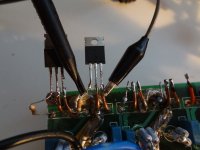
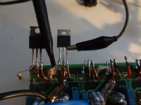
This picture shows two gate voltage measurements, once with the ground connected like this:
DSC01263.jpg
and once like this:
DSC01264.jpg
More than 1V drop just across that ittie-bittie piece of wire ! But... 20V drop across 84nH of inductance means it only needs 4nH for a 1V drop. The inductance
calculator I linked to earlier predicts an inductance of about 6nH per cm for the FET legs, so.... it all fits.
 
To build some understanding of whats happening and how to deal with the spikes I'll try different suppression techniques.
To see in more details whats going on it's usefull to run simulations in parallel with the measurements, as the simulations
allow to observe a lot more variables (like currents, power dissipation in components etc).
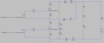
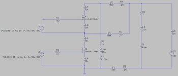
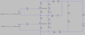
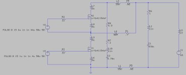
View attachment 13
I've added the 5nH inductance per FET leg and a 1uH inductor in the 65V power supply line. The 470nF capacitor has an 11nH
series inductor and a 1 Ohm series resistor to model its parasitics. The capacitor I use has part nr. 495-1298-ND from digikey.
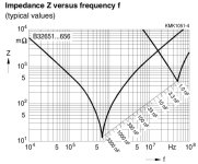
If you look at the datasheet it has this picture in it:
capacitor.jpg
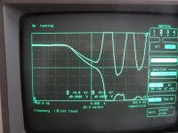
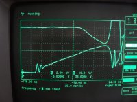
The resonance frequency (the dip in the graph) is at around 2.2 MHz, hence the 11nH inductance I added (using the resonance
frequency equation posted earlier). The series resistance should be about 50mOhm, but I upped it to 1Ohm to make the
resonance damping in the simulations more realistic...

The first thing to typically try is to add a big capacitor across the supply, but close to the FETs.
with_cap.jpg
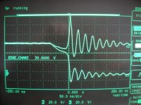
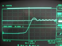
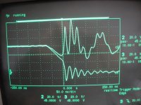
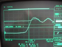
The measurements for current going into the controller (so the low side FET has the control over the edges):
DSC01275.jpg
DSC01276.jpg

The pictures show both the rising and falling edges of the output signal, and the power supply.
Not a lot has changed with the original pictures from a few posts ago.. The ringing for the falling edge has a bit lower amplitude
than the original, due to the big cap accepting the current from the power line inductor L1/L3 (due to the stubborn diode). The series
inductor inside the cap messes things up though, it doesn't allow a sudden change in current (not without a big spike in voltage), so
the big ringing is still there.
Intesting to realise is that the ringing frequency has not really changed, and that the big capacitor at the ringing frequency actually
acts as an inductor (because the impedance of the inductor at the ringing frequency is much higher than the capacitor impedance).
At 40MHz 470nF is about 8.5mOhm, wile 11nH inductance is 2.8 Ohm.
So, as the cap behaves as an inductor, all it does is reduce the total ringing inductance a little bit (it shorts out part of the 84nH wiring
inductance), which slightly raises the ringing frequency.
Simulations are in accordance with the measurements, so a big cap: not very usefull....

Next thing to try: a small capacitor across the supply:
smallcap.jpg
measurement results:
DSC01271.jpg
DSC01272.jpg
Now there seem to be two ringing frequencies occuring both together, one around 40MHz and the other at around 7 MHz.
I think the responsible parts are:
40MHz: 410 pF FET C_oss capacitance with L7, L8, L9, L6 and L10 series inductance
7 MHz: 4.7nF from C2 with L10, L3, L2 and L1 series inductance.
Simulations also show both ringing frequencies.

We can try to dampen the 7MHz component by adding a resistor in series with C2. 4.7 nF has an impedance of 4.8 Ohm at 7 MHz,
so at 1.5 times bigger the snubber resistor should be 7.2 Ohm.
snubres.jpg
View attachment 6
DSC01274.jpg

Some improvement but the big initial spike at low-side turn on is still there. The ringing is nicely dampened, I think if we can get rid
of the big spike the snubber across the supply line (at the FETs) is better than the single big cap.

The standard way of snubbing is to have a snubber across each FET:
standard_snub.jpg
measurement results:
DSC01281.jpg
DSC01282.jpg
Turn-on and turn-off seems to be slightly slower, probably because the snubbers need to be charged / discharged. The results
are not significantly better than when a single snubber is placed across the supply. The snubber across each FET takes relatively
large amount of power (f_pwm * C_snub * V_bat^2) while the one across the supply does (theoretically) not dissipate power. Therefore
the single snubber across the supply is prefered.

In all the shown cases here simulations are in correspondence with the measurements. So, experimenting in the simulator
makes sense !
 
One of the things the previous post has shown is that trying to force the spike at low-side turn on into a capacitor
doesn't really work due to the series inductance of the capacitors.
 
Ok I waited long enough... :) Sorry lebowski I waited as long as I could in fact I forgot about this thread but I was trying to clean up my inbox and remembered this from a couple PMs with you.
 
fine by me :D

I actually bought extra 4115's to build an output stage according to what I learned
due to / since this thread, hopefully I can post pictures and results in a few weeks :D
Going for a 6 FET with the FETs in 2 rows of 3, about 1 to 1.5 cm wide copper strips
for supply and some very narrow caps I found. No snubbers but minimising
power stage wiring inductances and bus-bar
 
Nice Lebowski, now venture into avalance land - that's where the magic happens :D

Edit: From joke to srs. Hexfets are in the middle between being snappy and soft. It is hard to compare MOSFETS since manufacturers use different testing regimens to find trr. If you find the time: try out some of fairchilds "shielded gate" mosfets. They are somewhat more fragile, but have better performance when it comes to rds on and switching.
 
Back
Top