It was a double pulse test of a half bridge with 2 parallel FETs on an inductor load, but not perfectly balanced. The end of the first pulse is on the left (turn off). I tried only this hard switching, was not interested in soft switching.
This is the Vds of the same test, measured also on the legs at the package:
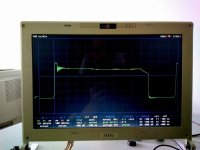
DC bus voltage was 64V, overshoot is 13V, and there is some ringing at 42MHz, 13Vpp. The total current was about 240A (just out of the range of a 200A ACS758 which tops at 220..230A).
The Vds edges are sharp (maybe too sharp), but the Id rise time is above 400ns - it appears on the Vds waveform as the chopped corner (L*di/dt) before the falling edge, and it is this long due to the high Qrr.
From where do you see it is EMI sensitive, by the gate ringing?
By your 475 and 575ns which transitions do you mean exactly, can you show on a waveform?
This is the Vds of the same test, measured also on the legs at the package:

DC bus voltage was 64V, overshoot is 13V, and there is some ringing at 42MHz, 13Vpp. The total current was about 240A (just out of the range of a 200A ACS758 which tops at 220..230A).
The Vds edges are sharp (maybe too sharp), but the Id rise time is above 400ns - it appears on the Vds waveform as the chopped corner (L*di/dt) before the falling edge, and it is this long due to the high Qrr.
From where do you see it is EMI sensitive, by the gate ringing?
By your 475 and 575ns which transitions do you mean exactly, can you show on a waveform?


