Controller builders: a gem about shoot through protection.

Teh Stork

1 kW
Joined
May 25, 2011
Messages
463
Since I do not have access to the wiki, I'll share my findings here.

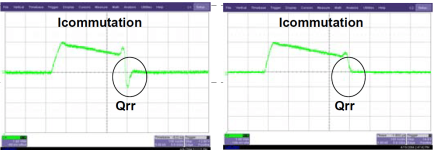
Setting shoot through protection is often looked upon as: "Increase dead time until power consumption goes down, and then increase this figure some - to be safe". The problem here is Qrr, or "Body diode reverse recovery charge". During dead time - the body diode will continue to supply current to the load. When the high side turns on, (this is rather hard to explain) the body diode of the low side mosfet is brutally stopped - This creates a huge spike and a lot of EMI with it.

My own experience; Reducing my dead time from 50nS to 18nS reduced TDH from 2% to 0,1%. It improved the efficiency of my controller from 92% to 94%! This was a huge source to EMI. This is one of the biggest improvements, and I wish it was the first I did. All the random noise problems was most likely much influenced from this. Qrr sets off hard switching ringing (this is a function stray inductances (layout and packages)). So, before snubbing your circuit - try adjusting your dead time. Choosing mosfets with lower Qrr could be a good way to go if that does not work.

Qrr varies with mosfet temperature, so care must be taken when optimizing dead time insertion.

Here is a bad graphic, but I hope it clears it a bit up.
Uten navn.png
 
Very cool. I remember we had a fellow on here to said he actually dialed in a tiny bit of over-lap, intentional shoot-through, for just a couple nS, and said it made a substantial reduction in freewheeling losses and system efficiency.

I didn't know what to think of that idea. What you've shown me helps me to understand it better.

Thank you for sharing your findings!

-Luke
 
I think I understand what you are saying but I gotta read up a little more to make sure I fully understand the concept. A 2% gain is pretty cool from just a simple change. Any downsides to this such as the time needed to be varied with temp?
 
zombiess said:
I think I understand what you are saying but I gotta read up a little more to make sure I fully understand the concept. A 2% gain is pretty cool from just a simple change. Any downsides to this such as the time needed to be varied with temp?

I made a drawing to try to make it easier to understand.

Uten navn.png

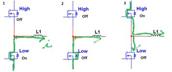
State 1: lower mosfet conducts, high off.
State 2: Both mosfets are off, inductor pulls current through lower mosfets body diode.
State 3: High side mosfet starts conducting, and in the process shuts down the lower mosfet body diode conducting. The diode (minority carrier) switches off quickly - causing ringing and EMI issues.

This is my understanding of it. You want to minimize the time spent in state two - without state 1 and 3 overlapping. Rise and fall times of both mosfets and gate drivers are influenced by temperature - so setting "perfect" dead time (or overlap for the best possible efficiency) must be controlled by the mcu. My controller has plenty of processing power left over - so I'm looking into if this is doable by some algorithm. Washing machiene controller employ quite a few temperature sensing resistors, but I've got no access to the code running on the controller.

I'm finishing my new controller, hopeing to reach 96% efficiency - bringing losses down to 200W at 5kW (the size of it all is like two credit cards right now). Running 100kHz-400kHz Pwm. The days of huge caps and 20kHz pwm are so last year :p One part of me wants to make this my bachelor project, but one part of me wants to make it into a open source project - we'll see :)
 
Teh Stork said:
I'm finishing my new controller, hopeing to reach 96% efficiency - bringing losses down to 200W at 5kW (the size of it all is like two credit cards right now). Running 100kHz-400kHz Pwm. The days of huge caps and 20kHz pwm are so last year :p
Muolto interesting. At what voltage are you running it and what MOSFET(?) turn on/off times are you having?

Teh Stork said:
One part of me wants to make this my bachelor project, but one part of me wants to make it into a open source project - we'll see :)
I'll cast my vote... OSP :)!
 
Njay said:
Teh Stork said:
I'm finishing my new controller, hopeing to reach 96% efficiency - bringing losses down to 200W at 5kW (the size of it all is like two credit cards right now). Running 100kHz-400kHz Pwm. The days of huge caps and 20kHz pwm are so last year :p
Muolto interesting. At what voltage are you running it and what MOSFET(?) turn on/off times are you having?

Teh Stork said:
One part of me wants to make this my bachelor project, but one part of me wants to make it into a open source project - we'll see :)
I'll cast my vote... OSP :)!

I'm running these very small mosfets. Turn off times are around 10ns to 16 ns, turn on times are around 7ns. Turn off delay are quite nasty when I charge the gate all the way to 10V (And the rds decrease isn't that big). With my current revision I increased the rise and fall times all the way up to ~120ns to make it stable. My next revision will run much tighter shoot trough (maybe even some ns overlap), and I hope this will make it stable with high frequency and high current.

All this time, I thought it was something other than Qrr frocking with my controller. As I've understood it, the reverse recovery charge sets off hard switching - and this turned out to be the root to so much evil. Now I want to find a way to optimize dead time, will probably blow up some more prototypes before I find a system ;P
 
Teh Stork said:
State 1: lower mosfet conducts, high off.
State 2: Both mosfets are off, inductor pulls current through lower mosfets body diode.
State 3: High side mosfet starts conducting, and in the process shuts down the lower mosfet body diode conducting. The diode (minority carrier) switches off quickly - causing ringing and EMI issues.
Let me start by saying Awesome!!

We need more people working on brushless motor control. We know batteries will be getting better and cheaper so lets be ready with the best motors and controllers possible!

Ok so I think State 1 and State 2 can't have arrows pointing the same direction other wise the power will just flow strait through the H bridge and cause a short. If you use the electron theory then electrons flow from negative to positive. So state 1 is correct. but State 2 would mean the Diode is going to stop the flow of power. But the induction of the motor will force current to keep flowing though the inductor it self until the field collapses. So what I believe happens is the electrons flow through different mosfet diodes. But I need someone to help explain this better because I am not a guru just always learning.
 
Arlo1 said:
Ok so I think State 1 and State 2 can't have arrows pointing the same direction other wise the power will just flow strait through the H bridge and cause a short. If you use the electron theory then electrons flow from negative to positive. So state 1 is correct. but State 2 would mean the Diode is going to stop the flow of power. But the induction of the motor will force current to keep flowing though the inductor it self until the field collapses. So what I believe happens is the electrons flow through different mosfet diodes. But I need someone to help explain this better because I am not a guru just always learning.

Remember, an inductor resists any change in current. So it will act as a lower voltage potential, allowing the diode to conduct. This is what happens in state two. When state 3 comes, the higher voltage potential will shut down the diode.
 
It took me a few read throughs to get what you are accomplishing, but that is awesome! I agree that controller hardware and software is a critical part of the next step in EVs, we really need more guys like you sharing your findings!


How do you like working with the dual cool package? I would love to see pics of the sandwich.
 
johnrobholmes said:
It took me a few read throughs to get what you are accomplishing, but that is awesome! I agree that controller hardware and software is a critical part of the next step in EVs, we really need more guys like you sharing your findings!


How do you like working with the dual cool package? I would love to see pics of the sandwich.

Dualcool, well - they have their pros:
- Very low package inductance
- Cheap, about 1,3 dollars a pop for 50.
- Source on top! (and Drain, Source and gate on bottom)

And cons:
- SMALL! 1 mm high, 5mm long, 6mm wide. Definitely easy to get them in backwards :(
- Hard to verify that it is truly well thermally connected when it is sandwitched down between two pcb's.

My pcbs with solder filled vias come in at around 4K/W, so cooling through pcb is possible. I used some copper bus bars first - they were nice, but hard to get all to line up and solder the way I wanted it to =/
 
Teh Stork said:
Arlo1 said:
Ok so I think State 1 and State 2 can't have arrows pointing the same direction other wise the power will just flow strait through the H bridge and cause a short. If you use the electron theory then electrons flow from negative to positive. So state 1 is correct. but State 2 would mean the Diode is going to stop the flow of power. But the induction of the motor will force current to keep flowing though the inductor it self until the field collapses. So what I believe happens is the electrons flow through different mosfet diodes. But I need someone to help explain this better because I am not a guru just always learning.

Remember, an inductor resists any change in current. So it will act as a lower voltage potential, allowing the diode to conduct. This is what happens in state two. When state 3 comes, the higher voltage potential will shut down the diode.
I agree with you on this other then the direction of current. I don't see how it can flow that direction though the diode. If current could flow that direction then it will just flow strait though the diodes in both mosfets in the H bridge and they will pop. I thought it flowed through the opposite fet diodes when they are shut off???? Kinda like when the speed of the motor is over the voltage of the battery and it pushes current into the battery. (this only happens on a steep hill or some rare instance which most will never see).
 
There are actually gate drivers that insert adjustable dead time by looking at the other fets state (If the other fet's gate is 3V, fet gate starts rising), but they are rather crude and I would like something more efficient. 20 ns are typical tolerance I find here, and I need 1-5ns. The search continues for a syncronous buck rectifier mosfet driver (Actually drivers designed for use on gaming motherboards have been the best match so far).

The main advantage with the Dualcool package (and every other low inductance package) is that you can switch fast and set off hard switching w/o huge spikes killing your fets. Just tried my 'old' To220 controller, damn it rings! :p

One thing I've come to realize by all this; ringing occurs between mosfets - and are not influenced by what load is connected to the power bridge.

And; redicolous idea nr 999: how about using distilled water as a heat transfer from copper pcb to aluminium case. 4 Oz copper with a surface area of 2 square inches comes in at 11K/W with a slight breeze over it. With water, this should be quite good. But then again - distilled water is a great solvent :S Coating the whole board in a light oil before adding water, I must try this :p

Just found this feature: Specified Miller plateau drive currents. How cool would it be if you could slow down switching when the load is heavy, and then have fastest possible at light loads? So much gate driver engineering porn (just hope it's not datasheet 'cool-aid').
 
This article is a must read for those of you building mosfet power stages.

Some quotes, that definitely had me thinking.

It is because the resistive voltage drop across the forward MOSFET and the layout inductance LSTRAY are the main factors limiting the speed of the reverse recovery process of the lower MOSFET's body diode. The optimal turn-on of the upper MOSFET is relatively slow and in most cases measures should be taken to avoid too speedy transition. This is particularly important if we realize that due to a low plateau level in modern devices the turn-on current of the gate driver tends to be higher than the turn-off current (and we want turn-off current to be as high as possible). Shifting to a more powerful gate driver will reduce the turn-off losses, but may actually make reverse recovery losses worse! With an unfavorable combination of factors this may lead to ringing at the gate of both MOSFETs, then multiple switching transitions, shoot-through and the destruction of the semiconductors!

Well, I had 5-6mm between Drain and source of lower and higher mosfet, so definitely too small stray inductance :roll: Also explains why I didn't see any ringing before my new driver killed itself, the frequency was too high.

A similar mechanism can be observed for the upper MOSFET. This time however the rapid rise of the drain to source voltage forces the transistor to turn-off in the middle of the turn-on process increasing the stress on the component.

The above phenomenon are not possible to eliminate entirely but have to be kept at a reasonable level. First we have to slow down the turn-on of the forward MOSFET. Luckily it is easy to do. We just have to put a resistor in series with the bootstrap capacitor. This will reduce the turn-on current without affecting the turn-off. We can also adjust the voltage of the upper MOSFET driver by selecting a small boot-strap capacitance. Second, let's not go overboard with reducing the layout inductance. It will take some burden of the forward MOSFET during turn-on. Third, use snubbers to slow down dv/dt (reducing coupling via Miller capacitance) and dampening the ringing.

This is also completely new information for me, and I'll have to look more into it to incorporate it into my design.

2. Reduce the dead time of the gate driver to minimum. It will decrease body diode conduction losses. If the dead time is near zero also the losses due to the reverse recovery of the body diode can be greatly reduced. In fact a small amount of shoot-through is the most efficient arrangement. Such precise adjustment however; requires gate driver timing varying with the load, input voltage, temperature, layout, etc. - an adaptive or predictive gate driver must be used. Luckily, integrated drivers of this kind are becoming available.

Just repeating it, since this is very relevant to the topic. I'm giving up making my microprosessor and "dumb" gate drivers time this (todays failure was the last drop). The piccolo series TI makes could probably do it, but I've got too used to programming with atmel microcontrollers. Even their ARM line can be programmed in C now :D Plan to explore the possibillity of using a ARM for FOC controll, possibly in conjunction with another microprosessor to ease the load on both. The bad thing is, by building a powerstage - I end up building a whole bike system xD
 
I think this is really interesting. Do you think it would work in practice, or is the deadtime sensitive to temperature and such? Have you been able to put a significant load on your design while running at >100kHz?
 
bearing said:
I think this is really interesting. Do you think it would work in practice, or is the deadtime sensitive to temperature and such? Have you been able to put a significant load on your design while running at >100kHz?

Well, my inverter works with this as of now. Eating 200A pulsed atm no problems (110A rms). The deadtime is sensitive to so many factors. Current across the mosfet, temperature. I use a XOR gate to detect cross conduction from high to low switch. If it is triggered - I enlarge the deadtime by 3ns. Opposite, if it is not triggered - I shorten the deadtime by 3 ns. This value can be negative. From low to high, I use a comparator. Same story here.

This means my gate driver hunts in on the optimum dead time. In normal operation it hits it dead on with ~1ns overlap or deadtime. It works as a control loop - predicting what the next switching event should be. With driving a motor, there are no sudden load changes - so it keeps the lock on the switching really good. There are two separate dead time/overlap insertions, both constantly being tuned, for each half-bridge.

dV/dt was a huge problem for me. It pulled my lower fet up when the top fet was switched on. So I had to slow the high fet turn on some, up to 40ns. Lower fet is about 20-30ns rise/fall. Having 6000A/us switching would not be possible without this predicting method.

100kHz is cake for the drivers and mosfets. Note that this would not be the case with TH technology. The package inductance of the PQFN is really small compared to TO220 or TO247. In my newest prototype I will increase the pwm to 180kHz inbetween 20 and 80% load - to lessen the strain on the decoupling capacitors.

The problem now is shedding the small heat this design makes. Cnc'd aluminum heatsink to connect to both top of mosfet and copper land area around them are in progress.
 
Hi,

I am building a brushless controller these days and read this thread with great interest.
Looks like have a major misunderstanding...
As I understand 3 phase BLDC drive there should be no shoot through current in a 6 step drive scheme.

Lets say high side MOSFET of phase A is turned on together with phase B low side FET, next commutation step should be (according to motor desired direction)
phase A topside MOSFET on together with phase C low side MOSFET.

After this phase C low side is turned on with phase B high side MOSFET.

There should be no scenario where the 2 MOSFETs of a motor phase winding change state in sequential steps only 2 steps apart.

I think the efficiency increase seen in this case is related to circulating currents when the MOSFET internal body diode circulates current during PWM off time.

Am I talking nonsense... :? ???

Thanks,
S.B.D
 
Some of the efficiency is lost in the Vf of the body diode, but since synchronous conduction is used, diodes will only conduct during deadtime.

But the big thing about the topic is that a diode cannot simply turn off. To make it turn off, some charge has to be removed, the "reverse recovery charge". On strong diodes, this charge is significant. If the MOSFET that is removing the charge turns on fast, then a big current spike will go through that MOSFET and the body diode. Since the MOSFET is only "half" conducting during that, the losses are big. The current spike will also induce ringing in the stray inductance between the MOSFETs of the halfbridge. The ringing is a cause of losses, and other problems too.

If deadtime is 0, the body diode won't turn on, so there won't be any Vf losses, no RRC to remove, and no ringing.

I use a XOR gate to detect cross conduction from high to low switch. If it is triggered - I enlarge the deadtime by 3ns. Opposite, if it is not triggered - I shorten the deadtime by 3 ns.

Interesting, but I don't quite understand.
What is the XOR connected to? the MOSFET gates? current transformers?
 
My mistake: I use a NOR gate, not a XOR gate. The system is quite complex, so telling every detail about it will be saved for when i have a comprehensive understanding of it myself, disregard what i said earlier - I'm not sure i explained myself correctly. As it is now, it uses too much processing power. (Or maybe I'll add a dedicated microprosessor to do this work). Adding a sample and hold circuit and more will make it easier. But under comes my 95% certain 'this works' setup.

The NOR gate is connected to gate-source and drain source of the lower fet. The gate-threshold is set to ~2v. The NOR gate should never go high. If both GS and DS is zero - that means we have a freewheeling mosfet (and NOR goes high). In turn, if NOR goes; deadtime is reduced. If it never goes high, deadtime is increased. This is the deadtime for the HIGH to LOW on transistion.

Then we have the LOW to HIGH on transisiton. Here i use a comparator sensing the lower fet. If body diode conduction happens here, drain to source voltage goes negative - implying that the deadtime is too big. If comparator goes high; deadtime is reduced. If it remains low; deadtime is increased.

This way; I have two different deadtime insertions. I have had many problems with EMI affecting my logic circuitry. My fets can do 70A fine, but bump it up to 200A - and things start to go apeshit. My controll method does not nullify body diode conduction - it still happens if very sudden load changes happen.

I also have a secondary system sensing the decoupling caps voltage - if they dip below a certain threshold; everything is shut down. When a shoot-through happens, decoupling cap voltage plummets very fast. The microcontroller can luckily react and shut down everything before anything is damaged. I've even tried delibirately shooting through to test this system, and it is surprisingly robust.

Saying "no ringing" is a exaggeration, but the ringing spike voltage is greatly reduced! Every fet bridge has some ringing on the transitions, the reason someone produces clean scope pictures is that the ringing is far out of the frequency of the scope. I experienced this when i reduced my rise time - suddenly, no ringing :eek: Turned out, after swapping to a scope two magnitudes more expencive than my what I had: I had a huuge but slim 180V spike over a 100V fet. Modern fets can operate in these conditions, given that they're within their avalanche ratings - but it is certainly a risky area. Some of the power supply students I study with has a dc/dc converter having 75V spikes on a 20V fet, this works nicely. If it will work or not is only determined by testing, in my experience.
 
Teh Stork, I love your controller approach. I am looking for high frequency controller for some time now, as I have a couple of projects sitting there and waiting, as they, due to motor construction, simply can not run on PWM under 200 kHz.
Best luck to you.
Subscribed.
 
circuit said:
Teh Stork, I love your controller approach. I am looking for high frequency controller for some time now, as I have a couple of projects sitting there and waiting, as they, due to motor construction, simply can not run on PWM under 200 kHz.
Best luck to you.
Subscribed.

Thank you :)

Originally I wanted to run hubmotors more silently with higher efficiency, but I've read up on low L low R motors too ;) The problems I've faced are the small time constant. My current sensors (they handle +-200A) can be shunted to accept bigger currents (This is also phase current, 1,4x batt current). The slew rate of my current sensors are 3uS, so they might be a bit on the slow side for a fast outrunner :(
 
circuit said:
So I guess you are using ACS756 from Allegro. To get higher slew rate, I'd consider an old fashioned resistor-shunt + fast opamp.

That's correct. And that was excactly what I was thinking ;) Will definitely make a resistor-shunted controller after this one is bug free. The simplicity of the allegro sensors are so nice, they've been a blast to work with :p
 
Teh Stork,

I'm confused unless it's a different problem I need to solve. I run low inductance hubmotors that love to snack on controllers, and all but one new controller have always run hot with these motors. If the issue is caused by the energy delayed/stored by the inductors that needs to go somewhere when the switches turn off, wouldn't the lower inductance mean less energy is stored in the coils that needs to be dissipated in the fet diodes, or am I out in left field?

John
 
John in CR said:
wouldn't the lower inductance mean less energy is stored in the coils
no.
Before energy can be stored, it needs to be transferred. If there is not enough inductance, the energy hits a roof. The moment this happens, mosfet pops.
This is not a accurate representation, but just an understandable explanation for those who cant get it.
 
Teh Stork said:
The NOR gate is connected to gate-source and drain source of the lower fet. The gate-threshold is set to ~2v. The NOR gate should never go high. If both GS and DS is zero - that means we have a freewheeling mosfet (and NOR goes high). In turn, if NOR goes; deadtime is reduced. If it never goes high, deadtime is increased. This is the deadtime for the HIGH to LOW on transistion.

Then we have the LOW to HIGH on transisiton. Here i use a comparator sensing the lower fet. If body diode conduction happens here, drain to source voltage goes negative - implying that the deadtime is too big. If comparator goes high; deadtime is reduced. If it remains low; deadtime is increased.

Thanks for the explanation! I think I get it now. If the circuit has detected freewheeling on the last transition, it will decrease the deadtime on the next transition. If it still detects freewheeling, it will decrease the deadtime even more on the following transition. It will continue like this until it stops detecting freewheeling, and then increase deadtime one step to prevent shoot through. In "steady state" it will jitter between two adjacent deadtime values around the optimum.

How are you able to adjust deadtime in such small steps? fast MCU frequency?
 
Back
Top