Linear Tech 12-cell battery monitor/BMS

kfong said:
Patrick, how about using silicone caulk from a caulk gun. That should have the pressure needed to flow down the channel.

Thanks - you were right. In the end I selected a non-acidic cure COTS caulk fit for a gun. Cost 1/10th the price and worked killer.


dbaker said:
Beautiful and it works great as well! For the silicone you might find a bead on the outside of each leg works as well as a much larger amount underneath the resistors. The resistor bond would then be in shear. Adhesion to the board is often not a problem.

Thanks to you too sir - After some testing I found this to be a much more effective method then filling a big blob under the resistors. In the end I ran "rails" down the PCB for each row of resistors. The legs of the resistors landed in the "rails" and squished out a little. I then ran a Q-tip down the sides to smooth the bead. I also ran a bead along the top to tie them all together like one large mass and then baked them out in the oven. Came out great - not a single problem yet.

Now... This is not to say that there have not been problems :)

I have 3 units sitting here on my desk that are missing (or at some time have lost) their magic smoke. To be clear - none of these were "mysteries" - all had a clear cause and effect - sometimes a long time in the finding - the cause being either me or the customer in all cases.


1) My prototype - burst into flames at one point when I ran it at 150V 20A without letting the PCB cleaner evaporate completely. I have since rebuilt this (several times) and it is still in service

View attachment 001_Methods_BMS_V3.0_Smoke.jpg
002_Methods_BMS_V3.0_Smoke.jpg
View attachment 3

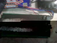
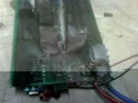
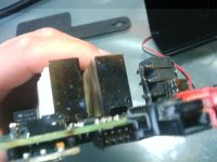
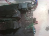
2) Not to be outdone - the customer sent me the pictures below. After a lot of head scratching the root cause of this failure was finally discovered... and it was a real good one! So very sneaky... The Charge leads and the Pack leads were inadvertently swapped. This means that instead of my IRFS4115 fets acting as PWM switches, their body diodes acted like heaters! The body diodes on these fets develop 1.2A and the customer was charging at 25A !!! That is 30W in a 1cm square area :shock: :shock: :shock: Needless to say everything was baked out including the (ever so important) conformal coating. The BMS actually completed its charge and then later - after a valiant effort - vomited its charge wires and died. Actually - it really is not bad at all. The BMS is still fine, only the charge fets and ceramic caps have to be changed out.

001_Customer.jpg
002_Customer.jpg
003_Customer.jpg


3) The third was the inevitable "miss-wire" where (it at first appeared) that the balance taps were plugged in out of order. It later was found that they actually were *not* plugged in out of order - but actually a freak accident occurred where the balance taps got crushed into a parallel adapter board which shorted out a bank of 5 cells. Long story short - a few channels got damaged but the BMS still works and needs only minor repair.

But... That is just the fun stuff :roll:

I have learned a TON along the way and I have quite a few tips and tricks. I am keeping the details of those to myself - but in the spirit of open source, here are a few VERY IMPORTANT tips that I will share with you.

1) Manually shut down all shunts before you take your A/D reading. Just shut them all off, poll the A/D's, then turn them back to whatever state they were in. Yea, yea ... I know the LTC will do this for you - but if you do some testing you will find that you can greatly improve your S/N by doing this.

2) For the LTC6802-1 you must do the above - here is why: The built in function to turn off the shunts is not aware of how many LTC chips you have in series. This means that when you try to read cell 13, the second LTC has no way to tell the fist LTC to turn off the shunt on cell 12. You either get what I am saying right now or you dont. If you dont - hit the books. If you do, then you understand how important it is to address this issue. Any time an A/D sample is taken you must turn off that shunt + the shunts above and below your sample

3) Turn off any PWM that you are running when you take A/D readings. TRUST ME... :| Your S/N will go WAY up. I have an algo that basically monitors the state of the charge PWM and turns off the PWM when a critical measurement is taken. When PWM is at 100% - obviously there is no need. On the other hand - once you are balancing.... You may find that you go into oscillation with your shunts if you are not getting really accurate readings. To give you an idea - I now balance to 2mV. Yea - thats right -> 2mV on a 25S 80Ah pack.

4) Really, really, pay attention to the noise you are creating with any PWM circuits. Switching 100V @ 25A is no joke -> That is 2.5Kw, thru many feet of inductive cable, and from a capacitive source. This can reap insane havoc on your switching system. In the end I solved the problem by throwing >10uF of 250V ceramic capacitance at it. This circuit was an electrolitic destoryer!

5) Design your prototype for rework.... use chip sockets for any dip parts, dont bother populating unimportant circuits, dont conformal coat, etc.

6) Use an acrylic conformal coating if you plan to re-work. Use a silicone conformal coating once you are confident.

7) Keep tight control on your firmware versions! Now that I have 3 versions of the BMS out there and a 4th in the works it is REALLY IMPORTANT that I send out the correct firmware updates. Really - the three versions are not compatible in any way - especially since I swapped to the -1 between versions 2 and 3. I have a TON of different versions out there for different applications too - some for dyno testing, some for troubleshooting, some for assembly checkout, some for my car specifically, some for...... Keep them straight and keep them safe!

Ok - that is the extent of the bad. :D
The BMS works beyond my wildest expectations and I could not be more pleased. Sure I had to do some hacks - but those are easily fixed with a PCB spin. All and all - things are working out splendidly!

Below I will post some fun pictures.

-methods
 
I am not selling these to the public.

If I ever get the money to do an ebike version it would look very different. I would do 12S modules that daisy-chain in a much smaller housing with a very small fan. I would probably eliminate the entire USB interface (to save power) and just have the system work stand-alone.

There are a lot of aspects to this design that make it undesirable for ebikes - not the least of which is its huge size and high price tag.

I am actually going *bigger* with the design for the next version. We are going to integrate more features into the housing and increase the charge handling to 150V 50A. That is what my batch of IRFB 4115's is for that I am sharing in the For Sale section.

-methods
 
fechter said:
methods said:
I have 3 units sitting here on my desk that are missing (or at some time have lost) their magic smoke. To be clear - none of these were "mysteries" - all had a clear cause and effect - sometimes a long time in the finding - the cause being either me or the customer in all cases.

Those look like pretty impressive burns. That's how you learn :wink:

Yes, that PWM stuff really raises hell with all sorts of things. At least you have the option to turn off things during the measurement. Trying to maintain accuracy to within a few mV with kilowatts of noise flying around is difficult.

Anyway, looks like you're making progress. Very nice 8)
 
I have been paying for my education alright :wink:

I have a lot of experience with firmware and electronics but I am definitely still learning about power engineering. Lately I have been trying to wrap my head around heat-sinking requirements. Luke has been helping me to try and estimate how many fets and how much heat sink I need to do a completely passive system. When you add the 50A 4khz PWM to the mix the power handling requirements go thru the roof! I think we have a handle on it and I am going to start building prototypes soon. Unfortunately with V3.0 I never had a lot of time to prototype so I ended up having to modify the circuit after the PCB's were spun out.

Having the option to turn off the Shunts and the PWM makes all the difference in the world at the last stage of balancing. Once all the cells are around 4.18V (as you know) just about any balance circuit will go into oscillation if there is any kind of noise. I chased my tail for a few weeks until I figured that out.... My shunt display used to play like a ghost piano. :p

I was looking at your latest creation..... Looks like you are using a similar zener approach to protect your TC-54 chips. I was not aware that you were popping those but it makes sense. I know you are the cheapest bastard on the planet so those zeners must really be necessary or you would not have them.....

-methods
 
Ouch.... Built an 18S 10Ah pack for a ride with a new Space Monkey and something went wrong... I think I might have actually reversed cells for the first time. After charging for 30 minutes the lowest cell was at 1.5V. Now after about an hour I am still not even up to LVC :(

The two packs that were low were HOT HOT HOT :shock:

001_FUBAR.jpg

Ignore the cells above 18
19 and 20 are short circuits, 20 - 25 are open circuit

-methods

EDIT: By "Went wrong" I mean that I did a crappy job building the pack. Nothing happened with the BMS - there was no BMS - As it obvious from my results :roll:
 

Attachments

  • Thrashed.jpg
    125.8 KB · Views: 707
Wait... are you saying the goal isn't to run your LiPo cells down low enough to reverse cell voltage? :twisted: :twisted: :mrgreen:
 
:mrgreen:

It is official - for the first time I have ruined lipo cells out of pure nOoBieNess :eek:
I think I might actually put a BMS on my "loaner" bike now :p

-methods
 
I have stopped reading PM's from people asking for help on the LTC.

On a brighter note - I have been patching up those units that were damaged in the field. The protection circuitry worked great - on one unit I only needed to replace a 100 ohm resistor and on the other I need only to replace the PWM circuits. Isolating each section of my board was a wise move in hind sight..... Did not lose a single LTC in all that carnage :wink:

The vertical mount shunts are still good too - no failures yet.

My only real complaint is that I tried to stuff everything into such a small box... Makes rework a living hell :(

-methods
 
hi all.
I'm heizal from Malaysia.
actually I'm beginner in battery management system currently do project using LTC.
I would like to ask a question.
>May I know what is the ideal voltage different between each cell so that can start doing discharge for balancing all the cell?

tq
 
heizal said:
May I know what is the ideal voltage different between each cell so that can start doing discharge for balancing all the cell?
0V
 
I hope someone can help me.
1) what is allowable tolerance of voltage between each cells so that it can be balance? the voltage variation rapidly change and if 0V difference to be balance the cell, the discharge operation will do continously.
2) when stack more than 1 board, I found that the voltage reading in second board is different. Voltage reading is lower than actual. Is it my firmware design wrong?

Hope someone can help me as i'm beginner in this field.
TQ in advance
 
heizal said:
I hope someone can help me.
1) what is allowable tolerance of voltage between each cells so that it can be balance? the voltage variation rapidly change and if 0V difference to be balance the cell, the discharge operation will do continously.

Damping

0V is fine - but your circuit will just be under damped or in oscillation
Anything greater is also fine - it will just drive your accuracy - right?

How about 20mV?

I do 3mV.... But then I also do a lot of things to make sure I take good readings - things like turning everything off while my A/D's are settling.... Taking the naive approach will result in very noisy readings (i.e. allowing the LTC to control the shunts while you take readings). I turn them all off manually -> Resulted in significantly less oscillation.


heizal said:
2) when stack more than 1 board, I found that the voltage reading in second board is different. Voltage reading is lower than actual. Is it my firmware design wrong?

Hope someone can help me as i'm beginner in this field.
TQ in advance

You need to include a lot more information here.... but right off I would guess you have a grounding issue between the boards. Could be firmware, could be hardware, could be wiring. My guess is that you are rigging together demo boards with too long of a ground lead. Is is just cell number 13 that reads low or 13 - 24? If it is 13 - 24 it would probably be a firmware issue right?

Think it thru and include all of the details. You will know that you included enough detail when you answer your own question before finishing the post :)

-methods


P.S. From that WIKI -> this is what you want.

Critical damping (ζ = 1)

When ζ = 1, there is a double root γ (defined above), which is real. The system is said to be critically damped. A critically damped system converges to zero faster than any other, and without oscillating. An example of critical damping is the door closer seen on many hinged doors in public buildings. The recoil mechanisms in most guns are also critically damped so that they return to their original position, after the recoil due to firing, in the least possible time.

In this case, with only one root γ, there is in addition to the solution x(t) = eγt a solution x(t) = teγt:[2]

x(t) = (A+Bt)\,e^{-\omega_0 t} \,

where A and B are determined by the initial conditions of the system (usually the initial position and velocity of the mass):

A = x(0) \,

B = \dot{x}(0)+\omega_0x(0) \,
 
Is is just cell number 13 that reads low or 13 - 24? If it is 13 - 24 it would probably be a firmware issue right?

-> all second boards cell connected (13-24) will read low reading. i also suspected something wrong with the firmware and will check again
thanks for your explanation.
 
Hi Method,
I detail my question.
I'm using DC1393B and DC590B board (programmed with own firmware).
The first DC1393B is connnected with 4 cells and second board DC1393B also connected with four cell (the connection as in Datasheet DC1393B page 3).
Connection between 2 boards are as in Configuration D Daisy chain SPI communication (refer to Datasheet Dc1393B page 12) with all the jumpers on the board set correctly.
The voltage reading for each resisitor connection is about 2.8V.
Then I run the firmware, each cell in first board shows 2.8V (same as actual), however in second board all cells shows only 2.6V each(lower than actual which is 2.8V).
 
Beware - the latest version of the LTC6802-2 demo board has a retarded mistake
Schematic

The inductor BLM31PG330SN1L is inline with cell 12+ between the cell and the shunt so if you want to make a *real* bms and not just a demo board you had better move that 33ohm inductor behind the shunt...

unless you want a BMS that does X amps on every cell but only 100mA on cell 12 :)

My V4.0 is ready for fab. All the fans and silly shit are gone. I am now using TO126 two ohm shunts in potted slave assemblies. Each slave does 4S-12S and has 2 RTD's. Slaves terminate in an 8" 25 pin flat flex cable that can be fitted with a custom board per customers request. Lots of cool new features.

I am no longer contracted by the company that asked for version 1-3.... this is a totally new and improved version that looks/acts/feels/is a totally new product. I will start a new thread soon.

-methods
 
Methods, isn't that part no BLM31PG330SH1 It's a ferrite bead, with 33 ohms at 100MHz, DC is 0.01 Ohm. I thinks it's an RFI/EMI filter for motor/load "trash" on the power line to the LTC part. Did you find it influencing the balance currents?

Congrats on your new design. Wishing you all the best with it!
 
bigmoose said:
Methods, isn't that part no BLM31PG330SH1 It's a ferrite bead, with 33 ohms at 100MHz, DC is 0.01 Ohm. I thinks it's an RFI/EMI filter for motor/load "trash" on the power line to the LTC part. Did you find it influencing the balance currents?

Doh - you are right. I just read 33 ohms in the BOM and made a poor assumption. I moved it out of the balance balance route anyway .


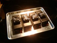
Here are some pictures of a slave unit. Final form will be a 1"x1"x4" block of epoxy/Aluminum with 20cm of flat flex coming off of it. The block will have to dissipate about 120W peak so it gets bolted to the frame. It can be run without additional heat sinking and ballance currents will be limited from 2A down to whatever can run while keeping the LTC below 85C.

The other end of the FF is where the water tight connector housing sits.

Yes I am aware that the FF is only 30awg. That is fine for 2A - especially with the insulator these have - and I dont take measurements while the shunts are active - so I dont have the accuracy problems that Gary and Fechter have to deal with. I am running 100 ohm resistors inline as it is.

-methods
 

Attachments

  • IMG_20110217_115501.jpg
    IMG_20110217_115501.jpg
    38 KB · Views: 1,759
  • IMG_20110217_115549.jpg
    IMG_20110217_115549.jpg
    40.9 KB · Views: 1,759
  • IMG_20110217_120248.jpg
    IMG_20110217_120248.jpg
    60.7 KB · Views: 1,762
  • IMG_20110217_120406.jpg
    IMG_20110217_120406.jpg
    47.7 KB · Views: 1,759
  • IMG_20110217_120448.jpg
    IMG_20110217_120448.jpg
    54.9 KB · Views: 1,762
  • IMG_20110217_125415.jpg
    IMG_20110217_125415.jpg
    51.6 KB · Views: 871
Very, very nice! I take it you routed the board and can get all the traces off pins 1-22 of the LTC chip? The ones close to the edge of your board.

I like how you are getting rid of the heat. We have only 3 options, convect it with air; conduct it with liquids or conduct it into structure. When you get small in electronics, heat is the problem. Just like fuel cooled avionics in high performance aircraft, the heat has to go somewhere or you are toast.

The one thing I don't like about the LTC part is if you re-power it, it resumes the factory default until you reprogram it. I heard there was a potential dash number revision being considered that would read state information from an eeprom... but don't know for sure it will be introduced. I also wish the pins were on 1mm intervals in lieu of the 0.5mm.
 
bigmoose said:
Very, very nice! I take it you routed the board and can get all the traces off pins 1-22 of the LTC chip? The ones close to the edge of your board.

This is actually the first PCB I have ever made totally on my own so yea - it is routed - but I used the AutoRouter. I set up an LTC ground and a communications ground on the second layer. I have two autorouting profiles - first one runs only grounds and punches a via as close as possible to the pin. Second one routes all the rest starting with the wides. I have 3 classes - 24mil for the shunts, 10mil for power, 8mil for signals. All chosen pretty arbitrarily - and I know the shunting traces are going to get quite hot. I did the calculations for a 60 degree temperature rise on a 65C ambient board and it worked out good enough.


bigmoose said:
I like how you are getting rid of the heat. We have only 3 options, convect it with air; conduct it with liquids or conduct it into structure. When you get small in electronics, heat is the problem. Just like fuel cooled avionics in high performance aircraft, the heat has to go somewhere or you are toast.

Well - I tried the surface mount and radials and found that they both were totally useless unless spec'ed at 20W or blown constantly with a fan so this is the next logical step. The TO126 are 20W and at 85C they derate to 9W which is about the peak that I can run them at. So long as I can keep the aluminum below 85C I can run at full power - but even 1/2 power is 5X the balance current of most systems so it will be fine.

bigmoose said:
The one thing I don't like about the LTC part is if you re-power it, it resumes the factory default until you reprogram it. I heard there was a potential dash number revision being considered that would read state information from an eeprom... but don't know for sure it will be introduced. I also wish the pins were on 1mm intervals in lieu of the 0.5mm.

I dont understand what you are getting at here - so you are going to be putting it to sleep by powering it down? The sleep mode on these is pretty good - what in the 10uA - 100uA range? Yea... I guess that with a smaller pack that could be too much - but it wont take but a few hundred uS to reprogram it each time you wake up and over time that wont even add up to 1uA.

The way I am using the chip I am pretty much constantly sending it commands and I have it set up to use the 2 second watch dog in case the uC dies. I dont really care too much about the power it eats up while sleeping - the packs I am working with are 80Ah.

-methods
 
I love the TO-220 shunt choice.
Huge improvement in thermal path.

Good work! I'm proud of you!
 
Back
Top