low inductance output stage contruction

Lebowski

10 MW
Joined
Jun 27, 2011
Messages
3,412
Location
beautiful Zurich, Switzerland
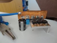
I;ve been walking around with an alternative method of building an output stage for some time now. After all the programming
I did for the controller IC I wanted to do some old fashioned soldering so yesterday I decided to implement my output stage
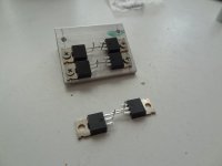
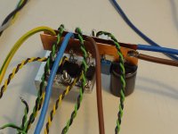
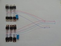
idea. Before I start with the idea behind it and the explanation, first a teaser picture of the result :)
DSC01370.jpg
The construction is a result of the learnings of my 'output stage musings' thread. Which can be summarised to "limit the power
supply inductances as much as possible".
The explanaition assumes the use of center aligned PWM, but I think it's also applicable to the standard china controller type PWM.
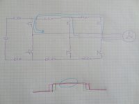
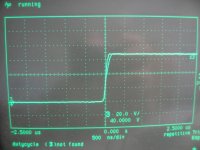
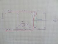
DSC01368.jpg
The bottom of the picture shows the center aligned output stage voltages. In the picture they start of 'low', then the 3 signals transition
to 'high' and back again. The different transition moments is what actually provides the power to the motor. But a large part of the
time all three output stage signals are either 'low' or 'high'. The schematic in the picture shows how the motor currents effectively
run around in a circle through the high side transistors and the parasitic power line inductances. The motor is assumed to have a
relatively high inductance, meaning the motor currents are constant (but yes, they have a triangular shape but the amplitude of the
triangle is low w.r.t. the average motor current).
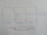
DSC01367.jpg
This picture shows the other half of the PWM cycle where all low side transistors are switched on. Note that the motor currents
have not really changed, they still flow in the same direction but now they all take the path through the low side transistors and
the parasitic inductances of the negative power line.

It is important to realise that first all the currents were going through the positive power line inductances, and now they are flowing
through the negative power line inductances. An inductor is an energy storage element, just like a capacitor. After the motor currents
stopped flowing in the positive power line inductances, these inductances 'dumped' their energy into the FETs, in the form of a
large voltage spike. And similarly for the negative power line inductances, when the currents are transferred to the positive power line the
inductor's energy will be dumped in the FETs in the form of a voltage spike.

The inductances that matter are the ones inbetween the three output stages, as these carry the full motor currents one half of
the cycle and no current at all the other part of the cycle. The motor current, except for the triangular ripple, stays constant. And
in the case of a sine wave controller, also the battery current is constant. The only real switching currents are between the three
output stages and the power line caps. So an output stage should keep these inductors to a minimum.
 
keeping inductors to a minimum, this is where bus-bars come into play.
The classic method is to use beefed up parallel traces or a thick copper wire soldered onto traces.
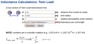
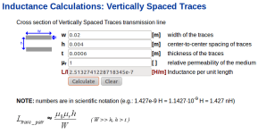
To get an idea of the inductance of this you can use the inductance calculator here:
http://www.technick.net/public/code/cp_dpage.php?aiocp_dp=util_inductance_calculator
For the classic traces:
parallel line.png
the result is about 630 nH per meter.
For a bus bar:
busbar.png
Only 250 nH per meter, a much lower value !

So, to minimise the harmful power line inductances first of all a bus bar type setup is much better than the classic
thick parallel wire. And second of all, as the inductances are per meter, KEEP THE POWER LINES SHORT !!

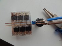
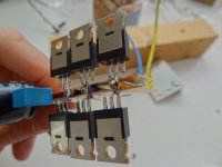
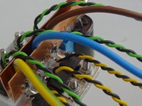
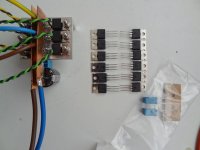
I decided to build my output stage based on these two points.

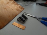
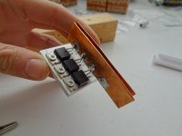
DSC01357.jpg
DSC01358.jpg
DSC01359.jpg
DSC01360.jpg
DSC01361.jpg
DSC01362.jpg
DSC01363.jpg
DSC01364.jpg
View attachment 3
DSC01370.jpg
DSC01366.jpg

In one of the picture comments I mention the diode/resistor combo in the gate driver lines.
DSC01369.jpg
When for instance a motor current is switched from the high side to the low side (with the current flowing into the controller), the
current is transferred from the high side freewheeling diode to the low side FET. To limit the reverse recovery current (reddish pink color) through the
diode it's better to limit the turn-on speed of the low side FET, and use a high gate resistor. Turn off though has to be faster
(and the gate must be kept 'strongly' to ground), needing a low gate resistor. This is achieved by using the diode as shown in the
picture.

Note also that the reverse recovery current flows through the power line inductors, and will switch off suddenly after the reverse
recovery time. Again, to limit the energy spike from the inductors the inductances must be as low as possible. And since the current
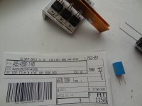
comes from the caps, these must be close to the FETs (see also the picture where the little blue block cap is soldered closest to the
FETs).
 
All pictures above are for a small 6 FET output stage. But what i we want more current to the motor and want a 12 FET or more ?

As mentioned before, the key is to keep the energy spike from the inductors as small as possible. The amount of energy is given
by 0.5 * L * I^2 .

The classic method for building a 12 FET output stage puts two FETs next to each other.
DSC01371.jpg
What you get is a construction which is twice as long as the 6 FET. This means the bus bars are twice as long, and with the
inductance being per unit length, the power line inductances will double. And, since we're going to 12 FETs instead of 6, it
is safe to assume the currents will also double.
When you plug the double inductances and double currents in the equation for the energy, you can see the energy becomes
8 times higher. When this is dumped it is dumped (for a 12 FET) into 2 FETs instead of 1 (6 FET case)
So, each FET has to deal with 4 times the amount of energy spiked into it ! Not good.

This is why I think it is better to separate the 12 FET into 2 6 FET stages and star connect towards the motor and power supply.
DSC01372.jpg
This situation is shown in the picture above. From each 6 FET stage the motor wires and power wires are connected to a
star point with equal length wiring. The motor and supply current will divide equally between the two 6 FET stages. For each
6 FET stage the current and power line inductances will be the same as for the original 6 FET case, so the parasitic energy
dumped into the FETs will be the same (and not 4 times higher !!)

It is however a different setup that we are used to. I think though my reasoning makes sense and that it will a better more robust
design. When building a 24 FET, it seems natural to build three half-bridge stages with 2 times 4 FETs in parallel, and use long
power line wiring between the 3 bridges. It is however much better to split the 24 FET into 4 separate complete 6 FET stages, and
use equal length wiring to common star points....
 
So, I'm trying to understand all the "fuzz" about inductance.

Inductance comes from the magnetic fields created around the conductor when current is flowing, correct? The magnetic field will "delay" the current since the current will need to build up the magnetic field before it really starts to flow. That's also why we need to put capacitors close to the FET's, so the capacitors can feed them with power until the current starts flowing from the battery, after the current have finished creating the magnetic fields around the battery wires. Please correct me if I'm wrong.

So inductance goes down the closer your power lines are spaced, according to the calculator in the link. Is this because the current in the power lines, runs in opposite directions and the magnetic fields created around the conductors cancel each other? And the closer the magnetic fields are, the more they cancels each other?
Then if you for some reason would attach one power wire to one end of the bus bars, and the other to the other end, the currents would flow in the same direction, "amplifying" the magnetic fields and we get a lot of inductance, is this correct?

I see you have twisted gate-source wires, they seem pretty long. I was told to keep them short, or well, keep the loop area small, is that what twisting them does? Sorry if gate lines are not the exact topic, but high currents are also flowing in the gate-source connections, and we want to keep inductance low in those too.
 
Futterama said:
So, I'm trying to understand all the "fuzz" about inductance.

Inductance comes from the magnetic fields created around the conductor when current is flowing, correct? The magnetic field will "delay" the current since the current will need to build up the magnetic field before it really starts to flow. That's also why we need to put capacitors close to the FET's, so the capacitors can feed them with power until the current starts flowing from the battery, after the current have finished creating the magnetic fields around the battery wires. Please correct me if I'm wrong.

So inductance goes down the closer your power lines are spaced, according to the calculator in the link. Is this because the current in the power lines, runs in opposite directions and the magnetic fields created around the conductors cancel each other? And the closer the magnetic fields are, the more they cancels each other?
Then if you for some reason would attach one power wire to one end of the bus bars, and the other to the other end, the currents would flow in the same direction, "amplifying" the magnetic fields and we get a lot of inductance, is this correct?

I see you have twisted gate-source wires, they seem pretty long. I was told to keep them short, or well, keep the loop area small, is that what twisting them does? Sorry if gate lines are not the exact topic, but high currents are also flowing in the gate-source connections, and we want to keep inductance low in those too.

for the impact of power line inductances, have a look at http://endless-sphere.com/forums/viewtopic.php?f=30&t=49450

the job of the power line capacitors is to shorten the effective wiring length / inductance. Without caps you would
need to take the inductance of the long battery wires into account. The caps short out this wire close to the output stage,
effectively removing the long battery wiring / inductance from the equation.

Exactly, the twising of the wires in the gate lines keeps their inductance low, and also reduces the magnetic coupling to the large magnetic fields from the motor currents
 
With my next build I was going to build 2 powerstages with 4 fets parallel then maybe try exactly what you show. I wanted to compare that to running 2 separate sets of windings in the motor as well.
 
nieles said:
awesome Lebowski!

how does it handle under load?

wish i had more time to work on my controller project.

I'm using it now with my development PCB, to write the code for the new controller IC. I've had it upto 10A phase
current at 65V supply, so not a real proper test yet for 4115's. But I want to make a PCB for the controller IC
including power supply and gate drivers, and then use the above described setup for the output stage. The
real test will come when I build the controller for my recumbent, which will run at 100V and 32 A phase....

Unless someone beats me to it of course ! I would love for other people to try this output stage setup.
 
Lebowski, I was planning to use this setup just to get my motor running so I can get a part-way success to keep me going on my build.

Now that you mention power supply, what is the common approach for powering the gate drivers and MCU? I have been working a bit with a LTC3630A and was originally planning to use one for 15V for the gate drivers, and one for 5V for the MCU, but I have also seen someone using a linear regulator to power the MCU from the 15V gate driver voltage. But if the MCU is a bit current hungry, the regulator would have to dissipate a good amount of heat.

Also, I have no idea of the power consumption of the gate drivers, this must depend on a lot of factors as well, like PWM frequency, MOSFET gate charge and number of MOSFETs. So I don't even know whether the 500mA the LTC3630A can deliver will be enough.
 
I think the LTC is a good choice, if your main battery voltage is below its 75V or so limit...

The gate drivers don't take that much current. An IRS2186 takes about 0.5mA for itself (if I read the datasheet
correctly). In addition comes the current from the gate charge which is given by f_pwm*Q_gate for each FET.
So, all in all 10 to 20mA is all the gate drivers take. The controller IC takes about 200mA from 5V.

In my controllers I have one DCDC going from 80-120V down to the 15V for the gate drivers. From this 15V
a second DCDC makes 5V. I use proper DCDC converters, not linear regulators because you're correct, the power
dissipation would be too high.

Making the 5V from the 15V instead of the high battery voltage has the advantage of either less ripple on the
5V supply or you can use a lower inductor value...

P.S. about the 30F4011, there are two versions, 20 and 30 MHz, you need the 30 MHz !
 
Ahh, DC/DC from 15V to 5V makes good sense. The 100V ceramic input capacitor for the LTC is not cheap, so not needing 2 of them or a higher value 100V capacitor is more cost-effective.

Lebowski said:
P.S. about the 30F4011, there are two versions, 20 and 30 MHz, you need the 30 MHz !
Correction: It's not MHz, it's MIPS :wink: and thanks, but I did notice that when I ordered so I got that covered 8)

Speaking of MHz, what kind of oscillator are you using in your controller IC? I don't see any crystal or external oscillator in the schematic and I don't see any internal oscillators in the 30F4011 datasheet so how does that work? (sorry, I should really move this question to the controller IC thread to keep this thread clean, I will do so later).
Edit: Ahh, the internal oscillator on the dsPIC is called FRC and the one for 30 MIPS must be 7.5MHz FRC w/ PLL 16x (120MHz OSC). I'm used to the term INTOSC for the internal oscillator :roll:
 
I think all dsPICs have an internal oscillator which can be used with its PLL. I have used one with a 7.3728 MHz int. osc, which could be multiplied with the 16x PLL for almost 30 MIPS. It looks like this part has a 7.5MHz int. osc, so it will hit 30 MIPS with the PLL.
 
Nice picture hack, I had to look three times :D

It will however not solve the higher inductance you get when making the whole
structure longer for parallelling FETs. You still have all the motor currents running
between the phase wires, first in one copper busbar plate and all switching over to
the othe busbar plate in the other half of the PWM cycle. The caps don't help against
this, however artfully you arrange them.
 
Lebowski said:
Nice picture hack, I had to look three times :D

It will however not solve the higher inductance you get when making the whole
structure longer for parallelling FETs. You still have all the motor currents running
between the phase wires, first in one copper busbar plate and all switching over to
the othe busbar plate in the other half of the PWM cycle. The caps don't help against
this, however artfully you arrange them.
Circular arangement? Disk shape controller. :D
 
Lebowski said:
Nice picture hack, I had to look three times :D
You inspire me :)

Lebowski said:
It will however not solve the higher inductance you get when making the whole
structure longer for parallelling FETs. You still have all the motor currents running
between the phase wires, first in one copper busbar plate and all switching over to
the othe busbar plate in the other half of the PWM cycle. The caps don't help against
this, however artfully you arrange them.
I see what you mean. I was only having in mind the spikes from the Irr through the caps ESL.

Concerning the "split it into several small power stages", the app notes from the manufacturers always stress we should have a good thermal "coupling" when paralleling FETs for better current sharing. You don't think that will be a problem?

As for the round controller, has been done, shouldn't be hard to find it around, Parabellum .
 
You are spot on Lebo. Might as well go all the way towards laminated buss bars. Lay some double sided kapton between your Cu foil layers and get them within 0.004 inches of each other.

Buss bar distribution I believe is required above a 5 to 7 Kw inverter level.
 
Lebowski said:
I;ve been walking around with an alternative method of building an output stage for some time now. After all the programming
I did for the controller IC I wanted to do some old fashioned soldering so yesterday I decided to implement my output stage
idea. Before I start with the idea behind it and the explanation, first a teaser picture of the result :)
View attachment 2
The construction is a result of the learnings of my 'output stage musings' thread. Which can be summarised to "limit the power
supply inductances as much as possible".
The explanaition assumes the use of center aligned PWM, but I think it's also applicable to the standard china controller type PWM.
View attachment 1
The bottom of the picture shows the center aligned output stage voltages. In the picture they start of 'low', then the 3 signals transition
to 'high' and back again. The different transition moments is what actually provides the power to the motor. But a large part of the
time all three output stage signals are either 'low' or 'high'. The schematic in the picture shows how the motor currents effectively
run around in a circle through the high side transistors and the parasitic power line inductances. The motor is assumed to have a
relatively high inductance, meaning the motor currents are constant (but yes, they have a triangular shape but the amplitude of the
triangle is low w.r.t. the average motor current).

This picture shows the other half of the PWM cycle where all low side transistors are switched on. Note that the motor currents
have not really changed, they still flow in the same direction but now they all take the path through the low side transistors and
the parasitic inductances of the negative power line.

It is important to realise that first all the currents were going through the positive power line inductances, and now they are flowing
through the negative power line inductances. An inductor is an energy storage element, just like a capacitor. After the motor currents
stopped flowing in the positive power line inductances, these inductances 'dumped' their energy into the FETs, in the form of a
large voltage spike. And similarly for the negative power line inductances, when the currents are transferred to the positive power line the
inductor's energy will be dumped in the FETs in the form of a voltage spike.

The inductances that matter are the ones inbetween the three output stages, as these carry the full motor currents one half of
the cycle and no current at all the other part of the cycle. The motor current, except for the triangular ripple, stays constant. And
in the case of a sine wave controller, also the battery current is constant. The only real switching currents are between the three
output stages and the power line caps. So an output stage should keep these inductors to a minimum.


Ok so I'm stuck thinking about this... Why is it better to do it this way? I mean if you have more fets in parallel for each phase in the same layout you have here the inductance across from one fet to the other in the same H bridge is sideways so the inductance is not a big deal.... Like my layout with 4 in parallel they are directly across from each other so the inductance from one fet to the other it needs to feed the current when one shuts off and the other in the same H bridge has to allow the diode to conduct to the caps is very low....
 
Arlo1 said:
Ok so I'm stuck thinking about this... Why is it better to do it this way? I mean if you have more fets in parallel for each phase in the same layout you have here the inductance across from one fet to the other in the same H bridge is sideways so the inductance is not a big deal.... Like my layout with 4 in parallel they are directly across from each other so the inductance from one fet to the other it needs to feed the current when one shuts off and the other in the same H bridge has to allow the diode to conduct to the caps is very low....

but going from one set of FETs to the other in the same H-bridge is not what matters. What matter is the power supply wiring
inductance between all the low side FETs in the three H-bridges, your layout for instance has long wiring between the 3 H-bridges
which is very bad for spikes. And along the same route, the same is valid for the power supply inductance between the 3 high side parts.

The power supply wiring between the 3 H-bridges in my layout is minimal for a 6 FET. For a 12 FET it gets double as long and,
combined with the higher current, you get 4 times the spike energy per FET...

The spike energy comes from wiring inductance where during one half of the PWM you have current flowing, and no current
during the other half of the PWM. When thinking about this you can assume the motor currents and current from the battery
to be constant.
 
Lebowski, this thread is currently my favorite alongside the controller IC thread 8)

I've got a new idea to a design for my power stage with your construction in mind. But I cannot get the inductance calculator to make the calculation.

Lets assume your busbars were 50mm wide, 5mm thick and spaced only 0.5mm apart. For the calculator, I get these values:

w = 0.05 (50mm wide)
h = 0.0055 (center-to-center should be 2.5mm + 0.5mm + 2.5mm where 2.5mm is half the busbar thickness)
t = 0.005 (5mm thick)
µr = 1

But the calculator says INPUT ERROR: Please check values.
 
Futterama said:
But the calculator says INPUT ERROR: Please check values.

You didn't provide a link, but I guess you are a using this one:
http://www.technick.net/public/code/cp_dpage.php?aiocp_dp=util_inductance_trace_v

Seems like you have to put h > 2*t for it to work. It's probably a bug in it's code, or in the help text. I wouldn't trust the value it calculates.

Anyway, nothing beats practice.
 
you know what i like about this test is that you are also using the heatsink to carry the current as did arlo. i hope to see both of your setups successful in the end proving out this concept. would be nice :)
 
HighHopes said:
you know what i like about this test is that you are also using the heatsink to carry the current as did arlo. i hope to see both of your setups successful in the end proving out this concept. would be nice :)
Almost there buddy :).
 
HighHopes said:
you know what i like about this test is that you are also using the heatsink to carry the current as did arlo. i hope to see both of your setups successful in the end proving out this concept. would be nice :)
As for as I can see, Lebowski is not using the heatsink as a conductor...
 
Back
Top