A Small 6 fet Vesc 6 Design

How can I find the correct value? I did a test of the voltage across the bootstrap capacitors on the gate drivers and they all measured 12v as expected.
 
Do I find the number of pole pairs by applying a current to two of the phases and counting how many positions the motor settles in when I turn it by hand?
 
Is there any way I can find the KV of the motor? I also attached a scope to all three phases and I am getting PWM across all of them. Maybe I can try openloop mode if there is any way to use it like a vfd where I can adjust voltage and frequency?
 
sdobbie said:
Is there any way I can find the KV of the motor? I also attached a scope to all three phases and I am getting PWM across all of them. Maybe I can try openloop mode if there is any way to use it like a vfd where I can adjust voltage and frequency?

For the motor kV you can use the scope. Just spin it and measure the frequency and amplitude then divide peak to peak voltage by erpm. If you want mechanical kV then you'll have to divide by pole pairs.

Try
foc_openloop 10 300
That'll spin with 10A at 300rpm like a VFD.

You might need to give it some inductance and resistance figures to calculate current loop gains though.
 
district9prawn said:
The formula to calculate flux linkage is 60 / (2*pi*sqrt(3)*p*kV) where p is pole pairs.

If I do this for my motor i get
60÷(2×3.14×√3×14×60) =6.566mWb. this is about what VESC detects (6.83).

But I understand 1Wb is one volt second and should be determinable by the integral under the sin wave if you spin the motor...

I get 1V amplitude at 60rpm 14pp is 14eHz... Period is 1/14s
So
1V/2 (for peak not peak to peak)
x 2/pi (for the area under a half sin wave compared to the rectangle around the half sin wave)
x 1/28 (half period to integrate under)
x 1/sqrt3 (for line to line to phase conversion)

Gives me the same result.

Is my derivation above correct?

Could you therefore just spin the motor on the scope and say the mWb is
0.5xVpp x half period x (2/pi/sqrt3)?
 
I follow your discussion about the flux linkage for a while now. I don't understand, why are you guys dwelling on such a sideshow?
This parameter is only important for sensorless run...

regards
stancecoke
 
stancecoke said:
I follow your discussion about the flux linkage for a while now. I don't understand, why are you guys dwelling on such a sideshow?
This parameter is only important for sensorless run...

regards
stancecoke
My experience in VESC is that getting it to run in pure hall sensor mode is tricky. It switches over after startup as soon as the observer appears to have locked.

Have you experimented with VESC? Have I been missing some option to shortcut the detection and just run?
 
So SDobbie sent me his controller to debug. Obviously I don't have a million other things to do, so I gave it a crack.

Fortunately, it was not a very long session, and I shall post some test results.

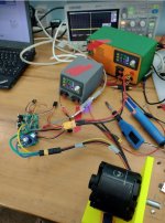
First, a picture of how I set it up:
XFOC setup.JPG
IMO, the design is somewhat annoying, having to have two seperate power supplies is a bit of a faff, but whatever, I have 2...
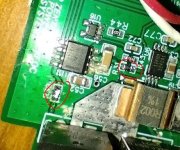
I had to solder a USB. The footprint was odd, I couldn't find a connector that fitted so in the end just fudged a ribbon onto it. Please populate the USB, they're only a few pence.

When I got it, it was pretty dirty. Soldering looked decent, but it was filthy, flux all over... Hosed it down with IPA and scrubbed it with an old toothbrush. Frankly i didn;t want to touch it before cleaning, it made my fingers all sticky :).

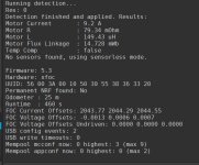
Now it gets better... No idea what firmware version it used and VESC currently has a fit if the rapidly changing tool and FW version are not the same so I went straight to command line...

XFOC detection params.JPG
Oh, it works, that was unexpected. Numbers are very reasonable for the motor (50kV Alien 80mm).

Maybe it won't spin up...
[youtube]oEjFULDfr-U[/youtube]
Oh, it did... :lol: Better than my one even!
XFOC foc_openloop 20 300.JPG

Let's take a look at the switching just for fun...
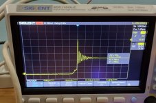
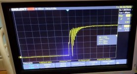
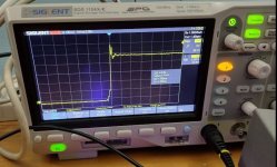
XFOC probing switch node.JPG
first, as it was, 10A phase:
XFOC 10A switch node 1R gate res.JPG
And the low side gate:XFOC 10A low side gate  1R.JPG

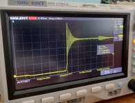
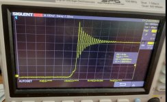
Not nice. Very not nice... The switching noise is quite bad.

Increase the gate resitor on one leg to 12R
XFOC mod to 12 ohm.JPG
XFOC 20A switch node 12R gate res.JPG
The noise is much lower, but still not good. I went up to 20R and there was a slight improvement but the turn on started to be too slow and it got hot very fast (think on the brink of shoot through)

Replaced with originals.


Now, this is where it gets interesting...
In doing this mod, i used the PSU for my soldering iron, which needs 12V.

Instant screeching as Sdobbie described when I plugged the board back in. I thought at first it was because fo my mods, but then realised when I turned the input back down to 9V all was well.

None of the rails are dropping out, just the current traces get horrid and the modulation increases from ~10% to ~60%.

I think the issue is just that there is so much noise. The ringing noise can be seen everywhere, on all the rails, all the... everything, and as you increase the gate drive voltage, it just gets faster and unmanageable. Or maybe there is something stranger I can't find, misconnections or whatever, things wired to the wrong voltage/...

Very surprised at this finding tbh.
 
Ecyclist said:
Thanks for testing it. :thumb:
I was wondering how good it can be. Obviously not great, but for $99 what can we expect :(

Let's be realistic, this is the first version sdobbie has made. Making something that works atall first time is bloody impressive. Every company/individual will have to go through this, sdobbies endeavour is just publicly viewable, and the speed from "let's have a go" to "here's a controller that spins up" is one of the faster projects I've seen on endless sphere.

The switch ringing is easy enough to solve, choice of snubbers, gate resistor changes, tighten the layout a bit. The squealing and not liking 12V on the gate drives issue will likely just go away with that, then shuffle a few connectors around and good to go.

I ran out of time to do any more on it, I have a hunch that if I find a way of feeding both supplies from the same PSU and swap out the regulator for a higher voltage more stable one and increase all 3 resistor legs, the problem might just go away.
 
mxlemming said:
Let's be realistic, this is the first version sdobbie has made. Making something that works atall first time is bloody impressive.

This is an accurate statement. Power electronics is not an easy field of study.

Have you tried to slow down the switching even more to see if it cleans up? Maybe try adding an oversized G-S cap, say 47nF. Sometimes with enough it will dampen the ringing. Have you figured out the layout inductance?

Your board cleanup might have done the trick, might have knocked loose a wire hair or solder ball. Good job helping him out.
 
zombiess said:
mxlemming said:
Let's be realistic, this is the first version sdobbie has made. Making something that works atall first time is bloody impressive.

This is an accurate statement. Power electronics is not an easy field of study.

Have you tried to slow down the switching even more to see if it cleans up? Maybe try adding an oversized G-S cap, say 47nF. Sometimes with enough it will dampen the ringing. Have you figured out the layout inductance?

Your board cleanup might have done the trick, might have knocked loose a wire hair or solder ball. Good job helping him out.

Glad to help him out. I shortcutted all these issues with my design by using ultra low inductance FETs so I'm actually finding it quite enlightening to experience the alternative first hand. I have to say I really was not expecting to find this much ringing, since the layout isn't all that bad (not great but I've seen worse work) and it's given me a whole new perspective on your previous comments on taming and slowing down the switching.

I can't slow it down any more easily without modifying the firmware to have longer dead time unfortunately, which is a faff. I can see how this would help by changing the Cgs and Crss ratio, as well as slowing it so I'll have a go at that but it'll have to be one of the later things.

Next thing I'm going to try is snubbers.

After that I'll try the capacitor but I'm also going to try swapping the FETs since sdobbie fitted it with really high current rated ones but they have a massive Crss and so are prone to self turn on and miller induced oscillation.

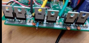
The inductance of the layout works out at about 6nH and so an optimal snubber mathematically is about 1 ohm and 3.3nF. I'll try that in combination with the 12 ohm resistor and see where that leaves me.
 
Wow, never expected it to be that easy to find what the issue was. It seems to be partly a layout and mostly a component selection issue. Agreed, ringing looks horrible and must be sorted.

I hope we can work out what mosfets are best for this design as well as work out a snubber. I take it the snubber goes on all 6 gate drive signals to the mosfets?

Thanks so much to mxlemming for looking at the design for me.

As everyone is helping so much with this, I can't in good conscience keep the hardware design closed source and market this all to myself so I think I will just open source my pcb layout so those with the experience can build their own and I can assemble and sell boards to people in my country who don't want the hassle of trying to build one.
 
sdobbie said:
Wow, never expected it to be that easy to find what the issue was. It seems to be partly a layout and mostly a component selection issue. Agreed, ringing looks horrible and must be sorted.

I hope we can work out what mosfets are best for this design as well as work out a snubber. I take it the snubber goes on all 6 gate drive signals to the mosfets?

Thanks so much to mxlemming for looking at the design for me.

As everyone is helping so much with this, I can't in good conscience keep the hardware design closed source and market this all to myself so I think I will just open source my pcb layout so those with the experience can build their own and I can assemble and sell boards to people in my country who don't want the hassle of trying to build one.

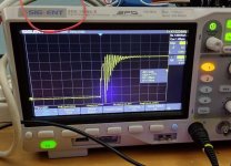
Few more things to test yet!

No need to open source it on my account, I've seen the design files already and have built plenty of my own ESCs. There's plenty of open source designs out there, the value adding thing really is that people can just buy it from you. No one wants to sit there soldering someone else's design, they just want to plug it in.
 
Had another quick go tonight, and I think this is as far as I am going to take this.

3 strategies:
1) larger resistors (12ohm drive)
2) add gate-source capacitance as Zombies suggests
3) Add snubbers (3.3 nF 1ohm was optimal... I could not find a 3nF and so used a 6.5nF)

I put one on each leg, so I could compare.
XFOC modifications.JPG

Without further ado...

Without treatment, the gate is horrid, and the switching can be seen in the post above.
Peak switch node overshoot is like 35V on a 24V bus voltage with only 10A. 5A gives some 22V overshoot.
XFOC VGS standard.JPG

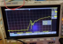
Larger resistors tame the ringing somewhat, but it is still bad. The gate traces are ugly, and the FETs get noticably warmer than no treatment and snubber treated. The most overshoot I could see at 5A was about 12V, so there is a measureable improvement.
XFOC Vgs 12R gate resistor.JPG
XFOC 20A switch node 12R gate res.JPG

Looking to the added capcitance, there is a small improvement. The Vgs is nicer, but the ringing is not really an improvement over the 12R gate resistor; they really are about comparable, though I did spot this one overshoot of some 25V at 11V gate drive:
XFOC Vgs 20nF gate-source capacitance.JPG
XFOC Switchnode with 20nF gate capacitance.JPG
(note this is at 11V gate drive voltage!)

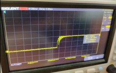
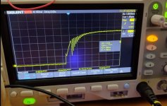
The snubber was overwhelmingly the best strategy here, with a vastly improved switch node profile, overshoot reduced to just 6V and no ongoing ringing. The gate profile was less improved, but definitely still better than with no treatment.
XFOC Vgs snubbed switch.JPG
XFOC Switch node snubbed.JPG

Doing this, I was able to bump the gate voltage up to 11.5V, with one different solution on each leg. I am confident by snubbing all 3 legs it would have done 12 or 13, as desired.

Overall, I recommend sdobbie:
1) Fits snubbers, use 1 ohm and 3.3nF for starters, and fit 0805 capacitor footprint and 1206 resistor footprint (0805 probbaly just OK if you pick higher power resistors).
2) increase the gate resitance to 4.7-12ohm
3) Consider adding a bit extra Cgs, certainly fit the footprint, but take care not to stack too much gate resitance and capacitance, or it will turn yuck
3b) I would guess 10nF and 4.7R is a good bet
4) Fit a higher voltage input regulator - the one used is only 15V rated, and add a regulator on the 12V line! If someone feeds it more than 12V, you might say byebye to it :).
5) Consider swapping for better FETs, the ones you have used, IRF100B201 are dino juice, . They have strong miller capacitance and that is what causes the nasty gate traces. Try FDP4D5N10C from On semi (available at RS now for 1.85 each).

Over to you dude, let me know if you want the board back, I have piles of high power boards now and so have minimal use for it!
 
Just noticed I've been posting rising gate and switch node when obviously these are not the same event. Should be rising switch node and falling gate, or vice versa.

It's not all that important, the results are the same just... Inverted. The gates still oscillate similarly and there's undershoot and ringing on the switch node as they fall.
 
If you don't have a need for the board, then I will pay your return postage to me.

Is this what I should start with? Hope I understood your suggestions properly.
Clipboard02.png
 
sdobbie said:
If you don't have a need for the board, then I will pay your return postage to me.

Is this what I should start with? Hope I understood your suggestions properly.
Clipboard02.png

You only need 1 snubber, C2 and R4.

This would be my starting point. You really need to look at it with the scope to see whether it's worked (do you have a scope?).

With the different MOSFET you might not need the 10nF atall (probably won't), but no harm in fitting the footprint.

The FDP has half the input capacitance of the irf100b201 so probably 10 ohm preferable to 4.7 ohm.

Perhaps swap out all the mos with the FDP and see what happens?

Re. Sending it back to you, happy to do that, just seems it might be easier for you to mod this one than build up whole new ones. I've honestly got more boards, motors, ebike bits than space to store them now, and this board needs you to fettle it before it's especially useful.

PM me your address, I'll get it posted.
 
The high side and low side are both snubbed by the low side snubber.

This is not especially intuitive, but the ceramic 1210s on the Vbus connect the GND and Vbus for high frequencies... They are essentially one and the same.

Another way of thinking about it is that the capacitors hold GND and Vbus exactly 24V (or whatever) apart. If there's no ringing on the low side, how can there be on the high side? The Vbus would have to be ringing synchronously.
 
sdobbie said:
How does this look? I managed to fit everything in.

Clipboard02.png

I'd aim to get c30 and r4 next to each other rather than inline but I think that's micro optimising.

Other thoughts I've had since are to give a bit of distance between the analog and power bits (the filters are all loopy next to the phase wires) and double check there's a solid dedicated ground plane.

In another thread we discussed issues with the ucc27211 and it's susceptibility to noise and accidental turn on (it's not meant for motor control, it's meant for high frequency buck converters).
 
Back
Top