peters said:
That was clear, but I wanted to add that another boards I have with similar inductances ring, so my conclusion is that low inductance alone is not the key to eliminate the ringing.
I think it is the added Cgs that makes a big difference if it is placed in a specific location, that's why I'm wondering where did you place it on your board?
(My layout is another story, I'll start a thread for that.)
Gotcha, we had some miscommunication.
I place my gate-source capacitance pretty much anywhere near the MOSFETs. I have not found location to play any role in my own testing. When paralleling devices I have tried one cap per MOSFET, a cap at each end of the traces and a cap right in the middle. The placement did not make any noticeable difference from what I remember, can't seem to find any notes I might have made on it several years ago, but I have a huge amount of notes on paralleling to dig through.
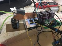
These are my notes on parasitics from my array of 11 paralleled TO-247 IRFP4568s I stumbled across which you might find interesting.
Measurements from apparatus #2
Natural ringing freq 10.0 MHz
Added capacitance = 0.96 uF
New ringing freq measured over 3 measurements = 0.658 MHz
Parasitics
4.2nF capacitance
61nF Inductance
Overlapped DC Bus area 18.88 in^2
0.01218 m^2
Capacitance per in^2 = 4.2/18.88=0.2225 nF
Inductance per in^2 = 61/18.88 = 3.2309 nH
Capacitance per m^2 = 4.2/0.01218=344.82759 nF
Inductance per m^2 = 61/0.01218=5,008.2 nH
I also agree that low DC bus inductance along doesn't fix it 100%, but it is key as the bus can't store much energy in the resulting magnetic field. Adding some additional G-S capacitance resolves a lot of the overshoot. I've also noticed it improves current sharing and works to slow switching time down when increasing the gate resistor doesn't provide the desired effect. With 2 paralleled devices and 10 ohm on/off resistors my natural switching frequency is <100ns on my most recent build. I found this surprisingly fast. Increasing to 20ohms made very little difference, but adding a 10nF G-S cap (measured at ~7.5nF) to one of the MOSFETs legs (I forgot to provision the PCB for a SMD resistor) provided very clean switching with very little turn off overshoot or ringing, better current sharing and D-S switching time of ~300ns. Downside is it increases power demand from the gate driver, but that is a non issue on my designs. In some of my previous G-S cap experiments I have observed that the amount needed to quell DC bus effects comes on suddenly. Adding 4.7nF to my current design made little difference, but going to 10nF made a huge improvement. Going to 15nF did not provide much additional benefit, neither did 20nF or 47nF other than slowing down the switching times.
bdj said:
Is your lauout with 6 lyers availbale on forum? From pictures how would you read rise time, time until reach full gate voltage or time until passes some value above treshold which provides me desired current?
Shouldn’t be surface of DC two copper plates be as big as possible because they form a very low inductance and resistance cap and provide start up current for switching process?
This is my most recent build:
https://endless-sphere.com/forums/viewtopic.php?f=30&t=106688
Inductance between two plates is a follows this relationship.
L = (u0*d*l)/w
u0 permittivity of free space
d = distance between plates
l = length of plate
w= width of plate
Good references:
http://www.nessengr.com/techdata/inductance/induc.html
http://www.pulsedpower.eu/toolbox/toolbox_inductances.html


