mxlemming
100 kW
- Joined
- Jul 17, 2020
- Messages
- 1,209
Hi all,
This is an educational post, because I was intrigued. Not the current state of the project.
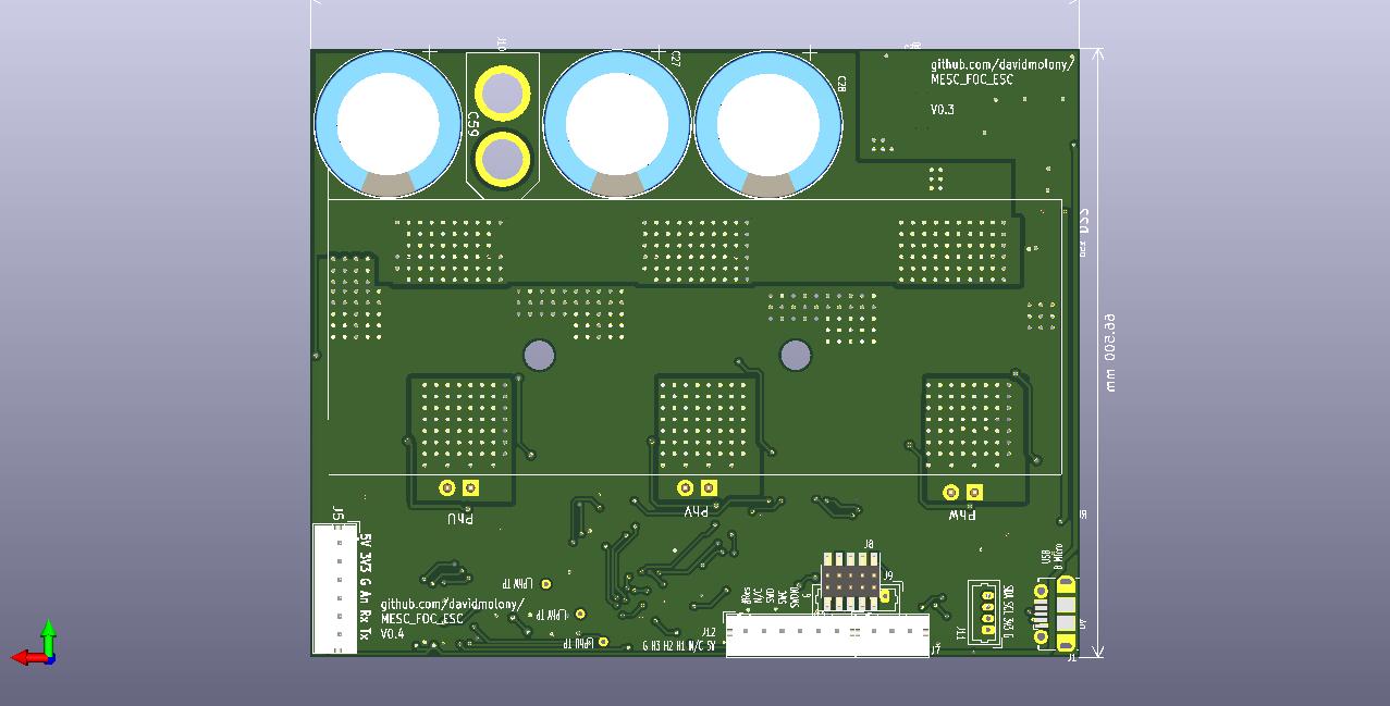
I have a few of the old version boards kicking about with D2pack FETs and snubbers. I wondered what the double pulse test was like for them.
Oh sheeet.....

Current was only up to 40A and voltage at 23V bus. The old version had 2x2mohm shunts paralelled for 1mohm.

The overshoot is enourmous on the rising edge of the old board!!

The undershoot is also pretty big on the old board...

Can't actually remember what the snubbers were, but I do recall they did very little.
This looks a lot worse than it is, because the bus voltage is small, and the current induced overshoot won't scale with voltage, but clearly 18V overshoot and 10V undershoot at 40A is absolutely miles away from the results of the other board.
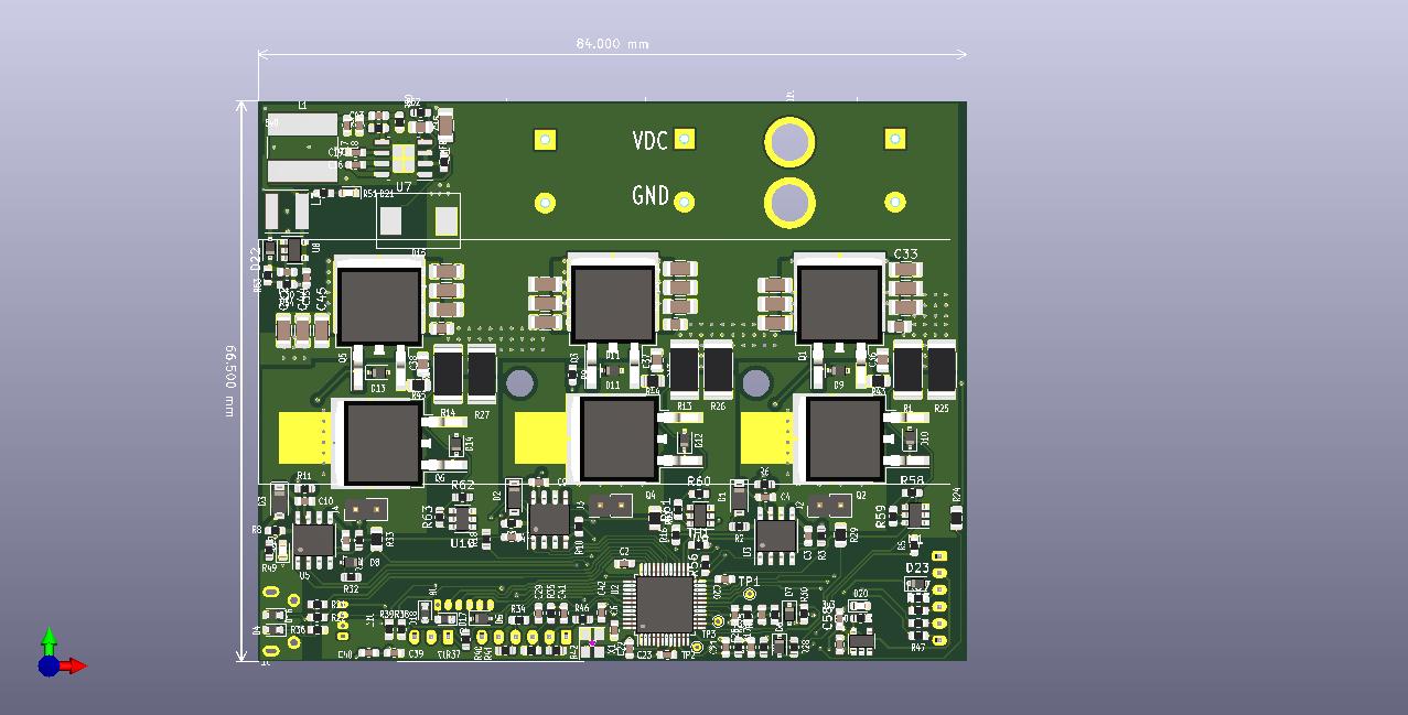
Perfectly workable actually given the target for the board was originally ~40A continuous, 80A peaks with ~15s (63V) safe, but the progress between this and the latest board is just stunning. A different FET package and a small rearrangement and the capability has more than doubled.
I rode this exact board to work for a few months, it's done hundreds of miles at 13s with no issues. I got 5 almost fully populated boards for like 65GBP (90USD) so the capability was already pretty great.
Regarding the new board:
I have a few ideas to get further improvement:
1) Remove the dual fit on the D2Pak. I think it's clear now that D2Pak is crappy compared to TOLL. This means I will be able to push everything a bit tighter still.
2) I can't particularly see why the decoupling caps need to be connected to the low side of the shunt. If I went VDC to shunt high, on a few of the ceramic caps at least, the inductive loop need not include the shunts. This might remove a decent portion of the remaining inductance. The difference between 1.5nH and 1.1nH perhaps.
3) Might be able to overlap the shunt high net and the VDC net a bit on an inner layer, which would eliminate some more.


I really am not sure this is worth the effort though given the previous results. I certainly won't be buying more boards to try it, but if Stancecoke's testing goes well (he's had one on his jig and spun it up...) perhaps there will be another order!
This is an educational post, because I was intrigued. Not the current state of the project.
I have a few of the old version boards kicking about with D2pack FETs and snubbers. I wondered what the double pulse test was like for them.
Oh sheeet.....
Current was only up to 40A and voltage at 23V bus. The old version had 2x2mohm shunts paralelled for 1mohm.
The overshoot is enourmous on the rising edge of the old board!!
The undershoot is also pretty big on the old board...
Can't actually remember what the snubbers were, but I do recall they did very little.
This looks a lot worse than it is, because the bus voltage is small, and the current induced overshoot won't scale with voltage, but clearly 18V overshoot and 10V undershoot at 40A is absolutely miles away from the results of the other board.
Perfectly workable actually given the target for the board was originally ~40A continuous, 80A peaks with ~15s (63V) safe, but the progress between this and the latest board is just stunning. A different FET package and a small rearrangement and the capability has more than doubled.
I rode this exact board to work for a few months, it's done hundreds of miles at 13s with no issues. I got 5 almost fully populated boards for like 65GBP (90USD) so the capability was already pretty great.
Regarding the new board:
marcos said:From the pics I think my board has at least 1/2 the parasitic inductance and stiffer dc link.
The low side shunt, wire bonding inside your fet, the caps arrangement, the stackup, they are all increasing your parasitic inductance. In my board miller is limiting both turn on and turn off swiching speed. In any case, looked acceptable so its running on the dyno now.
I have a few ideas to get further improvement:
1) Remove the dual fit on the D2Pak. I think it's clear now that D2Pak is crappy compared to TOLL. This means I will be able to push everything a bit tighter still.
2) I can't particularly see why the decoupling caps need to be connected to the low side of the shunt. If I went VDC to shunt high, on a few of the ceramic caps at least, the inductive loop need not include the shunts. This might remove a decent portion of the remaining inductance. The difference between 1.5nH and 1.1nH perhaps.
3) Might be able to overlap the shunt high net and the VDC net a bit on an inner layer, which would eliminate some more.
I really am not sure this is worth the effort though given the previous results. I certainly won't be buying more boards to try it, but if Stancecoke's testing goes well (he's had one on his jig and spun it up...) perhaps there will be another order!