Hi Neil,
Wow! What a dedication! Let me go through the questions you sent me:
The transformer winding numbers are quite arbitrary, I did not take the transformer apart, I do not even know the direction of winding although I could measure all that as soon as I have the supply working.
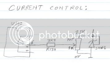
SHR2 is identical to SHR1, both are AZ431 voltage references (2.5V). You can think of them as a zener diode with a control pin or as a regulator. The control pin is compared to the internal 2.5V reference and if the control input is lower then the device does not conduct, if the control pin is higher than 2.5V then the device does conduct.
From the 48V positive, a line runs downward passing by R122 and then into a diode. The other side of the diode does not connect to U100 pin 6 but only to the 3k3 resistor that feeds pin 8 (power supply), The line from pin 6 crosses and does not connect to the diode and the 3k3 resistor.
The two paralleled switching FETs are N-channel.
The current shunt J100 in the negative 48V line is missing, it is located between the 3 680uF elcos and the 5k6 bleeder resistor.
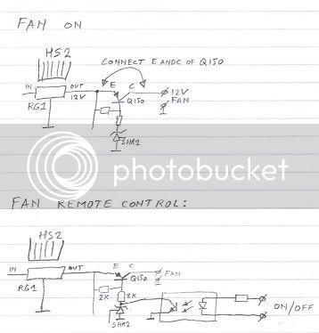
RTH1 and relay: this circuit looks perfect, the value of the resistor is 510 Ohms (sorry for my crappy handwriting).
The cap below it with the question marks is a safety and EMI reducing cap between the rectified AC negative and the secondary (48V) negative. Value is 2n2 250V~. The other side of the cap and the SVR1 top connection must connect to the -48V output near the LED, because where it connects now is at the wrong side of the current shunt J100.
Resistors R100 and R101 are 39 Ohms - again a case of my handwriting....
Note that L100 connects directly to the bottom of the lower secondary winding. The R101 and C101 are a snubber from the diode output to the negative 48V line (the bottom of the lower secondary winding)
The resistor feeding the base of Q5 and ZD2 is 3k9 in value (3.9 kOhm)
The pair of resistors from the Source of the switching FETs to negative supply, R56 and R both have value 0.22 Ohm. The reference nr of the other resistor is R57.
The two switching FETs are called Q1 and Q2. The 5.1 Ohm gate resistors are R10 for Q1 and R12 for Q2. The zener diode protecting the gate drive is called ZD1 (not ZN1) and the resistor parallel to the zener has value 5k1, I made a mistake in my sketch.
The marking that ended up under L100 is actually meant to be a voltage level indication at the junction of L100 and R127, here the voltage can get as low as -59mV at maximum current (voltage drop across the J100 shunt)
I think that is it - much less changes than I expected, you have done a wonderful job of capturing the schematic from the hand-drawn sketch that I sent you, thanks for all your hard work! Now people will be able to fix their NES if it blows up, mod them because they understand how it works and in general a lot more people will be happy with their NES because it can now be used just as easily as the 'S' series.
At the same time I do not think that Meanwell will have a problem with this schematic, even though it is an effort of reverse engineering, I deliberately left a few unimportant components off the drawing and most caps do not have their value noted down, so you can't build this power supply from the schematic - so the effect will be that the NES will be sold *more*, not less.

")