Designs for Reliable (low V) Cell Monitoring electronics

Alan B said:
This would seem to argue that resolution beyond 50mV would be useless when the motor was running?

I agree, Alan, under load the accuracy probably doesn't need to be better than +/- 50 to 100mV. However, to be really useful the unit needs to look at the likely load conditions, maybe indirectly, to try and deduce whether or not cells are being subjected to conditions likely to cause damage.

This is an area where the added intelligence that a ucontroller adds could be beneficial, by reducing the incidence of false LVC indications, perhaps by trying to separate out under-load conditions from no-load conditions and adapting the warning accordingly.

Jeremy
 
GGoodrum said:
Once permanently mounted inside a pack, I've never had one of the TC54-based LVC circuits fail, and I've built a ton of these since 2007. The only failures I've had were when they were initially mis-connected, or if a wire from the board to the cells broke/came off, but adding a 5.1V zener on each cell fixed the latter problem. With LiPo-based packs, I've never seen one fail yet, mainly because each 5Ah "sub-pack" comes with a pre-wired balance tap.

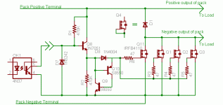
To get around the problem of the opto/ebrake not stopping a pack from killing itself, if a controller is left on, for instance, you could always add a very simple active cutoff circuit. The one below was originally posted here by a "brief" member, Randomly, and it works extremely well and has very little standby current drain.


I'm working on a very simple "BMS" for a 12V SLA replacement motorcycle/marine genset starter battery that will use a similar version of this circuit that will handle about 250-300A.

-- Gary

Thanks Gary, that wholly supports my view, based on my experience with high reliability measurement stuff over the years.

I'd forgotten about Randomly's contribution, pity he/she's not still around and contributing.

I can't help but feel that sometimes ucontrollers are seen as the solution for all problems like this, when the reality is that they are useful, but not universally so.

Jeremy
 
GGoodrum said:
Once permanently mounted inside a pack, I've never had one of the TC54-based LVC circuits fail, and I've built a ton of these since 2007. The only failures I've had were when they were initially mis-connected, or if a wire from the board to the cells broke/came off, but adding a 5.1V zener on each cell fixed the latter problem. With LiPo-based packs, I've never seen one fail yet, mainly because each 5Ah "sub-pack" comes with a pre-wired balance tap.

To get around the problem of the opto/ebrake not stopping a pack from killing itself, if a controller is left on, for instance, you could always add a very simple active cutoff circuit. The one below was originally posted here by a "brief" member, Randomly, and it works extremely well and has very little standby current drain.


I'm working on a very simple "BMS" for a 12V SLA replacement motorcycle/marine genset starter battery that will use a similar version of this circuit that will handle about 250-300A.

-- Gary

Glad to hear from you Gary, and that's good data on the reliability and failure situations. So the failure modes seem to be more related to the connection and handling process than the usage.

Interesting turn-off circuit there on the FETs. One question - doesn't this place the dying cell in the position of having to supply the optocoupler LED current to maintain the disconnect? In the controller left on in the garage scenario this would add the LED drain to the already dying cell, and as soon as the cell passed down through about 1.5 volts the disconnect would release and reconnect the controller?? Perhaps a latching circuit or relay should be added requiring a reset. The TC54/Optocoupler might actually contribute to the demise of the low cell by adding to its drain when it passes below 2.1 volts. Unless I misunderstand the design.
 
My experience with reliability in vehicular electronics started a long time ago when I built a voltage regulator for the generator on an old pickup truck. It was just a small fistfull of transistors, but the lesson was clear. Impedance is your friend. Placing the maximum amount of impedance on each interface to the outside world, combined with protection diodes or zeners and filter caps, makes the design far more "protected" against the inevitable misconnections, noise, spikes, and general junk that a real world device sees in a noisy environment. Semiconductors don't do well with high voltage or current spikes.

We cannot readily do this on the TC54 designs due to the requirement that the LED current must be drawn from the cell that is being measured. So this places the TC54 in a vulnerable position, with fairly low impedance to the battery.

Adding zeners is a great protection against connection in the wrong order. It will not protect against connecting to the wrong cell. This is consistent with Gary's experience where they don't fail while connected to a pack, but when being connected/disconnected incorrectly (where the presence of a properly wired connector reduces or solves that issue).

One question is whether the micro brings additional value by not having these weaknesses. It is more robust against user mistakes in wiring and system noise transients. It can also give some confirmation that the code is working and happy and that all cells are in their normal ranges, which is not present with the TC54.
 
Gentlemen,

Before you go too far, it might be worth a few calculations of the implications of working with 12 bit ADCs.
What resistor precision do you need in the potential dividers?
How many dB reduction in the electrical noise is required?

Nick
 
Actually, Randomly's original LVC circuit didn't use the optos. I think the current draw when the FET(s) were on was about 120uA, but that dropped to the 1uA used by the TC54 when tripped. Here is his original schematic, followed by his circuit description:

LVC-Opto Cutoff.gif

The circuit operates as follows-

Assume all the battery cells are at 3V, above the 2.1V cutoff point of the TC54 ICs. This means the output of all the TC54 are high.
At the bottom stage the high output of IC1 pulls the base of Q1 to 3V, which puts about 2.4V across the emitter resistor R1 creating a pulldown current source around 16 uA out of the collector of Q1. The next highest stage IC2 output is also high and pulls the base of Q2 up through D1 to 5.5V. The 16uA current pulls down on the emitter of Q2 turning it on and the current exits out the collector to the next stage above. The transistor Q12 is connected as a diode, and is reverse biased at this point flowing no current. Each successive stage continues to pass the 16uA current along, and you can insert probably as many as 30 stages. Any more than that and you will need to have fairly high Beta transistors to minimize the current lost to the base on each stage. With a high beta transistor you could probably take it up to 100 stages. Each stage re-uses the same current as the previous stage so quiescent current consumption does not increase with added stages.

Finally the 16ua pulldown current reaches the base of the PNP Q7 pulling it down and turning it on. Because Q7 is configured as an emitter follower the base is pulled negative until Q17 starts to conduct and clamps it to one diode drop below the ground of IC7. The output of IC7 is high and pulls R7 up to the cell voltage, 3V above IC7 ground. This puts 3V minus the diode drop of D6 across R7 and the 120uA flowing through it exits out of the collector of Q7 becoming a 120uA pullup current source which turns the output FETs on.

Now say IC2 detects a low cell voltage of 2.1V and it's output goes low. This removes the base drive from Q2 and the emitter of Q2 is pulled down by the 16ua current until diode connected Q12 starts to conduct and clamps the emitter voltage of Q2 at one diode drop below the ground of IC2. This keeps Q2 off since we have the extra diode drop of D1 in series with the base of Q2. This process shunts the 16uA current off into Q12. There is now no current pulling down on the base of the PNP Q7 and it turns off. R10 shunts any residual leakage currents and keeps them from turning on Q7. This same process works for any stage.

If the top stage IC7 detects a low cell voltage and pulls it's output low it also shuts off Q7 in a somewhat similar manner.

At this point you could just put in the 12V zener D7 to clamp the gate voltage and the pulldown R8 and connect it directly to the gate of the IRB4110.

However the turn on and off times would be quite slow, especially the turn off because of the very large gate capacitance of Q11. It's a bad idea to turn the output FET on or off slowly under heavy load as the power dissipation in the FET will be enormously high during the transition. With a 1000W load the FET will be dissipating 500W in the midst of the transition. A fast transition minimizes the time for the FET to heat up. To accelerate the turn on and off times I've added Q8-Q10 and associate components

To accelerate the turn on time Q8 is connected as an emitter follower to drive the gate. It amplifies the 120uA pullup current by it's Beta so for a beta of 100 the gate pullup current will be 12ma. It may be useful to use a darlington transistor for Q8 which would give you gate turn on currents more in the 0.5-1.0A range making the gate turn on under 1 uSec.

To accelerate the turn off Q9, Q10, D8, and R9 are configured in a positive feedback clamping circuit similar to an SCR. When Q8 is pulled high current flows through D8 and charges up the gate of Q11. As long as Q8 is on and pulls up R9 and the base of Q10, Q10 remains off (and thus also Q9). However when Q7 turns off Q8 also turns off and R9 now pulls the base of Q10 down and turns it on. The collector current of Q10 flows into the base of Q9 turning it on and the collector of Q9 pulls down even harder on the base of Q10 in a positive feedback loop. This rapidly discharges the gate capacitance of Q11 through the emitter of Q10 and slams it to ground. Once the gate voltage falls below 1V the SCR circuit stops conducting and it's ready to be pulled high again by Q8.

In this second pass I've gotten rid of the schottky diodes and some unneeded parts. All the parts are fairly non-critical. Just about any small signal transistor with decent beta at low Ic can be used for Q1-Q6, Q12-Q17. A beta of over 100 at 10uA would be good, 2N5962, 2N5088, 2N5089 is good if you need something in a T0-92 package. Q7 is also fairly non critical and just needs to be able to take the full pack voltage, a KSA992 is rated to 120v. A 2N7051 darlington for Q8 will handle 100v, and 1.5 Amp giving fast turn on times. SS8050 for Q9 and SS8550 for Q10 are good high current and cheap parts that will give very fast turn off times. D8 can be a 1N4001-1N4007 type.

The Quiescent current of this circuit is low. At full pack voltage when the FET is on it is around 150uA, as the cell voltages drop this will drop toward about 100uA. You can reduce this current further, down to less than 50uA, but at the cost of increased switching times of the gate of Q11.
When low voltage cutoff is reached and the circuit turns off Quiescent current drops to about 10uA for those cells below the cell that tripped the circuit. For the cell that went below the 2.1V thresheld the current drain drops to 1uA (the quiescent current of the TC54). All the cells above this also have their current drain drop to 1uA. Any further cell that hits it's LVC threshold also has it's current drain reduce to 1uA.

Because of the active output drive the turn on and turn off times of the output FETs Q11 are very fast which protects Q11 from damage if it turns on or off into a heavy load.
This circuit will fully protect a pack, even if a motor controller or any other load is accidentally left on. If a discharged pack was left uncharged even for an extended time this circuit will continue to function correctly no matter how low the cell voltages fall and will not put any drain on the pack beyond the 1uA quiescent current of the TC54.

You can see Randomly's various posts related to this on this page: http://endless-sphere.com/forums/viewtopic.php?f=14&t=3345&start=330#p61712. In this ost, he shows how the active cutoff portion of the circuit can be used with the opto-based circuits. I didn't care so much about solving the "leave the controller on" problem, so I didn't use his full version. For most setups I was more concerned about providing the active cutoff function for standalone setups that didn't use the ebrake/throttle pulldown scheme. For our standalone 12V battery BMS, I will try the full "randomly" solution. :)

-- Gary
 
Thanks for digging that up, Gary. Good stuff to review and keep alive.

The garaged controller left on problem is a tough one. Especially if no one is around to hear any kind of audible alarm. Need a wireless connection, but it is not very practical. Chirping like a smoke alarm is very low power, but still requires someone to hear it. I hate to put all that current through another set of FETs just to solve that issue.
 
A couple of observations:

Your voltage dividers on the input will drain the batteries. Most uP ADC inputs are fairly low impedance or require low impedance loads (like 10K)... certainly more than a desired passive load of 1 microamp or less. Perhaps an isolation JFET on the divider inputs would work?

A 5V zener diode on the ADC inputs will go a long way for providing overload protection.

You can get very good resolution and accuracy by averaging lots of ADC samples (res improves as SQRT(number samples). My CD FET welder uses an AVR. It has a battery analyzer mode that samples the cell voltage 10,000 times a second. I get 0.001V res with a 1 second integration time. Also around 0.001V accuracy by software calibration (and I'm using the 5V supply for the ADC reference).

I am playing with a BMS design that uses a single 8-pin micro per cell. The BMS would be expandable in 8 cell slices. A 4/6/8 cell per micro is a possibility, but the micro per cell has certain advantages. The micros are not powered by the cells, but by a capacitively coupled clock driven by a master CPU. Cut that clock signal and the load on the cells is essentially zero. Another option is an AD7740 V/F converter on each cell that talks to a central controller.

The BMS would have an integral switched capacitor cell balancer for keeping the pack in whack.
 
This chip has differential ADC input capability that looks quite interesting for this application. It can do 8x gain on the differential inputs to counter the dividers. It looks like it can do this with either polarity on ADC0-6, so 7 channels. So all but one cell could be handled that way, making the resolution 4 millivolts rather than 32.

In terms of the input impedance, there is a trick to decrease the load on the cells of the divider. First of all, the 30:1 reduction helps some. The other trick is to make the input filter capacitor large enough. It then becomes the "source" of the voltage for the ADC, and the resistance of the divider can be raised to achieve the desired lowpass function.

The question is, what is an acceptable load current for the monitor?
 
texaspyro said:
A couple of observations:

Your voltage dividers on the input will drain the batteries. Most uP ADC inputs are fairly low impedance or require low impedance loads (like 10K)... certainly more than a desired passive load of 1 microamp or less. Perhaps an isolation JFET on the divider inputs would work?

A 5V zener diode on the ADC inputs will go a long way for providing overload protection.

You can get very good resolution and accuracy by averaging lots of ADC samples (res improves as SQRT(number samples). My CD FET welder uses an AVR. It has a battery analyzer mode that samples the cell voltage 10,000 times a second. I get 0.001V res with a 1 second integration time. Also around 0.001V accuracy by software calibration (and I'm using the 5V supply for the ADC reference).

I am playing with a BMS design that uses a single 8-pin micro per cell. The BMS would be expandable in 8 cell slices. A 4/6/8 cell per micro is a possibility, but the micro per cell has certain advantages. The micros are not powered by the cells, but by a capacitively coupled clock driven by a master CPU. Cut that clock signal and the load on the cells is essentially zero. Another option is an AD7740 V/F converter on each cell that talks to a central controller.

The BMS would have an integral switched capacitor cell balancer for keeping the pack in whack.

Be aware that those input protection zeners can cause a lot of grief with their leakage unbalancing the resistive divider. Have had that problem, would rather depend on the protection diodes in the chip with adequate series impedance.

I have made a few micro per cell designs but am not too happy with the parts counts.

Lots of interesting ideas. Capacitive balancers sound interesting.
 
Alan B said:
Be aware that those input protection zeners can cause a lot of grief with their leakage unbalancing the resistive divider. Have had that problem, would rather depend on the protection diodes in the chip with adequate series impedance.

Been there, built that. Tends to not be a problem. Certainly not at the required resolution level. Belts and suspenders are the way to go for reliable operation in harsh environments. Go with as high an impedance source as you can get away with with zeners (and filter caps) as backup. Zeners do have lower effect with lower impedance inputs. JFET isolation on the ADC inputs seems to be the most promising... I tend to eliminate the filter caps and depend more upon software averaging to tame noise... one less component to go wrong.
 
texaspyro said:
I tend to eliminate the filter caps and depend more upon software averaging to tame noise... one less component to go wrong.
You can often get undesired higher-frequency noise aliasing back into the inputs this way though. This can cause the signal levels to either be higher than they really are or the extra noise can be interpreted and acted on as being really there, i.e., part of the desired signal or voltage level you're reading. Averaging will only average out differences between two measurements of the summed signal+noise, not remove the effect of the unwanted aliased noise.

I never use an ADC without R/C filtering (or occasionally, active filtering) every input to limit the bandwidth of the signals/voltages. IMHO, the odds of the filter caps or resistors ever failing are fantastically low. Assuming that the inputs are otherwise protected from spikes/surges and other nasties though. If those inputs are not protected, the R/C filter failing is the least of the circuit's problems.

But, if things have been working well without filtering out the frequencies that you're not interested in, then they're not a problem! :mrgreen:
 
There's been a lot of discussion of the architectures that can be used for a BMS (circuit topology, component selection, etc.) but IMHO the architecture of a BMS is not the cause of BMS failures. It's either the lack of knowledge of how to spec the switching components (FET drivers and FETs) and the cooling "system" for the BMS or cost decisions. Hmm...add a few failures related to incorrect component value selection (too low a power rating, etc.) for voltage regulators in hi-volt BMS/controllers though.

BMS designers can easily create an incredibly reliable BMS any number of different ways, but that costs money and takes up more room. Market-driven decisions dominate the production of BMS (and controller) designs and this leads to failures. "Why keep the FETs cool? Most will survive heating beyond their rating for long enough". "Why use 5W resistors on the voltage regulator? The 2W versions will last long enough". "Why protect the circuit from bigger spikes, it works plenty well with our tiny test motor".

Understanding the ratings for the components that are selected, and applying those ratings conservatively will do more for BMS reliability than any function architecture IMHO. I'm not saying that we shouldn't look into proper overvoltage/ESD/spike/surge protection, immunity from cell connection order or connectors coming off randomly, etc., just that these are very high level decisions and don't ensure any kind of reliability if the components are under any kind of stress.

Just about any decent architecture/circuit topology can be reliable for years and years. It's the little things that can count for so much. I realize that this is just a personal soapbox rant...just had to get it out. :)
 
I agree with that last post, John. I can't help but feel this thread is beginning to look like a search to find a clever and complex way to use a microcontroller, rather than an effective way to build a reliable cell monitor. The way that the complexity of this simple task seems to be growing it looks very much as if this is turning into a 'sledgehammer to crack a nut' solution to cell protection.

I believe that a simple TC54 based solution will be more than adequate. It's simple, has been shown to work well and draws less current from the cells than their self-discharge rate, so is OK for long term connection to the pack. The only thing I'd change over the current LVC designs is a way to disable the LVC during pack storage, so that a cell low event doesn't cause more current to be drawn from the cell than the normal 1uA or so, causing accelerated cell damage.

What would be a far better use for the intellectual effort being expended on this (in my opinion) would be a foolproof capacity gauge. The Cycle Analyst does a pretty good job, but is very multifunctional and a little complex for a non-technical user. Something that gave an idiot-proof display of battery capacity used since last charge, with an easy to read display (preferably analogue, perhaps a bar graph, in presentation , for at-a-glance reading) would be very useful and probably save more battery packs than another BMS. If it were open source and used commonly available (and affordable) components, then that would be even better. I've been working on a very simple gauge, but to be honest it really needs more time and effort dedicated to it, by people familiar with newer ucontrollers and knowledgeable in writing good code for them.

Sorry if this is going off track, but I hope that it's in the spirit of the threads intentions - to protect cells.

Jeremy
 
I'd like to throw into the mix a recommendation to take a look at the existing gas gauges available on the market. I've mentioned this in other threads, and hate to sound like a bad recording here, but TI, Maxim, and others have already done a huge amount of the hard work needed to track capacity accurately.

I've had incredible success with TI's gas gauges (bq78PL114, essentially a one-stop-shop for BMS' modules up to 12S, stackable to any voltage). It has:
- Tracked capacity to better than +/-5% for charge/discharge current levels up to 5C/100C. To better than +/-2% for 5C/10C.
- Only draws 300uA.
- Includes active charge-transfer balancing operating during charge, discharge and rest.
- Has a built in 5-LED SOC display capability.
- Operates standalone (no microprocessor or firmware needed).
- Has incredibly flexible safety settings (almost 200 of them, allowing each user to tailor their BMS without rewriting firmware or using jumpers).
- Protects the cells from a huge range of potential problems.
- Can output a wide range of data for review via a serial port if desired.

Their line also includes single-cell gauges that can be used by stacking them up, optoisolating their serial ports, and reading each one via a micro to get the SOC for each cell. Not as elegant as a multi-cell chip like the bq78PL114, but more modular.

Using any of these off-the-shelf gas gauges lets the designer concentrate on physical implementation of the design (as I've mentioned earlier, IMHO the weakest point in most BMS') like the case, MOSFETs and cooling, and not worry about developing a huge amount of firmware. Some gauges are tied to just the list of specific cells they have developed configuration files for but others are "system side" gauges that are designed to reside outside the pack. These learn on the fly what the capacity of the cells are, some without even going through a complete charge/discharge cycle.

Just tossing out an idea. :)
 
CamLight said:
(lot's of very good comment, snipped for brevity).........

Just tossing out an idea. :)

And an exceedingly good idea it is too, John. I had a feeling there were some potential solutions to this problem out there, but to be honest hadn't taken the time to go and search for them as you have. They look like a good foundation to work with to me.

Jeremy
 
I updated post #1 based on what we have learned.

The TC54 does not meet the requirements outlined in post #1. Details are in post #1.

The CellLog does not meet requirements either, also detailed in post #1.

The goal of this design is to meet a reasonable set of requirements for a high reliability cell monitor, not use a micro. I have used TC54 type designs for 10 years in other projects.

The micro design proposed in post #1 appears to meet most of the requirements. Some requirements will not be met until more detailed design is done (such as power consumption). Are there any other proposals that meet these requirements?

Are there errors in the requirements?
 
One of the biggest challenges for a micro solution to this cell monitor is the power consumption. If we use a power budget of half a 5AH pack per year this puts a 285 uA maximum current from any pin.

The regulator has about 15uA quiescent current, and the micro is about another 15uA, so about 250uA is left for the sampling dividers.

The current through the voltage dividers is roughly 8+7+6+5+4+3+2+1 = 4*9 = 36 * 3.3/R = 120/R = 250uA, so R = 475K (resistance of each divider, min)

Alternately an FET might be used to turn off the sampling as was mentioned earlier, though that adds a lot of parts to the design.

If a lowpass filter having a DC input resistance of 475K and an AC output impedance with enough capacitance to charge the ADC input is used it should meet requirements.

The input capacitance of the ADC is 14pF, if we use 15nF for the external cap (1000x internal) then the time constant would be about 7 milliseconds.

This filter also provides a lot of protection for the ADC inputs.

My remaining concern is the level of input ADC leakage currents that might disturb the divider.

Edited to fix the math error mentioned below.
 
Alan B said:
The input capacitance of the ADC is 14pF, if we use 15uF for the external cap (1000x internal) then the time constant would be about 7 seconds.

1000 x 15 pF = 15 nF not 15 uF (BTW, I HATE nanofards, life goes from picofarads to microfards and skips that sucky nanofarad step). And electrogeezers don't do pF, they use uuF

Besides the input capacitance, you have the requirement to charge the ADC internal sampling capacitor... hence the recommended 10K input source impedance. You can get by with higher source impedances if you are only sampling one, slowly changing channel.

The main problem with TCxx cell monitor designs is they only work with fixed voltages. I want a design that works with any cell chemistry. Also a micro or ADC channel per cell architecture gives you both LVC and HVC protection.
 
Thanks for the math correction. Good catch. That's what I get for trying to do too many things at once here. I remember uuF, that was awhile back. Also high vacuum FETs with built in heaters. Lots of fun stuff.

According to the chip specs, 14pF includes the S/H capacitors and all sources of capacitance in the chip. So if we are satisfied with a 7 millisecond time constant, and if there are no significant leakage currents this technique should work. Leakage current specs show 0.05uA worst case which on 475k is 24mV. So that is on the scale of one bit, which should be acceptable.

A pair of quad op amps could also be used for buffering, or differential amps, but I'd like to avoid that if possible. It would also likely require power management on the op amps to stay within the power budget.

The FET approach takes quite a few parts as well, and likely puts the FETs at risk for transient damage, and it is difficult to verify for faults during operation. Self testing is a useful feature for something we want to know is working.

This approach with the low pass filter is not something I have tested yet, but it appears to be worth investigating. It is not difficult to build a circuit with a lot more components. The engineering challenge is to meet requirements (including reliability) with a small number of parts.

edited to fix the time constant
 
Tiberius said:
Can I ask again, what resistor precision do you need in the potential dividers?

Nick

Good question.

If we need 0.1V accuracy with 30V full scale that would be 1 part in 300 or 0.3%. Precision resistors have gotten fairly cheap these days. Especially if surface mount is used.

But the real issue is stability. We probably want to calibrate the ADC anyway. So in that case we need stability in the resistors, and calibration will compensate the values for the actual resistances.

If we want to use the differential mode of the ADCs then the resistors will have to be significantly better.
 
regmeister said:
I'm an electronics tech, but most of this discussion is beyond me. Eager to read along though.

I've been following a new chip architecture that looks promising for the BMS application and will share a link. Possbily some of you have seen it?

They have a pdf note describing their high impedance ADC which discusses how it has inherent noise filtering built in which will help reduce external component count and power requirements.

I see they've announced a 144 cpu chip to be released next summer, but I think their 4cpu chip or similiar would be interesting for monitoring batteries. In general the chips are being touted for super low power and high speed.

"ANALOG INPUT: The F18B analog to digital converter (ADC) is a high speed, free running counter that can be read as up or left using a special protocol. Its count down frequency varies between ï‚»3.6GHz for Vdd input and ï‚»5.7GHz for Vss, as shown in the typical transfer function at right. The vco ctl field of io selects mode as below, with counter disabled on reset to save power. A voltage is measured in the operating range (ï‚»750mV to ï‚»1.3v) by calculating the difference between two readings separated by a known time interval. To assist distribution of a time base for sampling and for driving digital signal processing operations, a node with an ADC is supplied with a phantom wakeup pin, always in input mode, used in cooperation with another node."

I'm guessing that anything with ghz frequency is not going to be low power enough. But who knows. Are they low in cost, too?
 
Back
Top