
You are using an out of date browser. It may not display this or other websites correctly.
You should upgrade or use an alternative browser.
You should upgrade or use an alternative browser.
Bafang M500/M600 thread
- Thread starter El_Topo
- Start date
Tomblarom said:@CiDi I see, but why would you have this at the handlebar? (I'm going to update the drawing, as we figured this out!)
Check the cable better, in the BMS connector there should be CH, CL and GND.
casainho
10 GW
- Joined
- Feb 14, 2011
- Messages
- 6,058
It may work as M365 motor controller, see:CiDi said:casainho said:Updated the EasyDIY display schematic.
The CTRL pin is put to GND when pressing the power button on the remote. Then there is a voltage divider with 2 resistors, to change the battery voltage to max of 3.3V (including a 3.3V zener diode as a protection) to avoid that signal to go over 3.3V, that is the limit of the microcontroller pin. The microcontroller will then read the power button state by reading the voltage with an ADC.
I would like to get feedback, does anyone things this is wrong? or suggestions for improving??

From what I could see, the P+ terminal that you call ctrl, is the same that is used to power the display, its voltate never drops below 2,2V.
The VCC terminal, has voltage only after switching on and I think it serves to power the usb socket.

VBat pin will only have battery voltage when the motor controller is enabled, and that way everything can be powered from that wire.
And the CAN logs messages you record for power on and por off, make all sense!!
For power on, we see display start sending the first commnds and only after a while, the motor controller sends the first commands (it may take a while to boot, as it may make some own checks).
Tomblarom
10 W
- Joined
- Jul 20, 2018
- Messages
- 93
I measured. Four times now and I'm 100% that the finding are correct and occouring on both versions. See the colors for reference:

Code:
   B8-F -- B3-F
3 [ylw] -- [blk] 1
8 [grn] -- [blu] 2
2 [red] -- [red] 3

   B8-F -- B5-F
6 [org] -- [org] 1
3 [ylw] -- [wht] 2
7 [brw] -- [brw] 3
8 [grn] -- [grn] 4
5 [blk] -- [blk] 5Tomblarom said:I measured. Four times now and I'm 100% that the finding are correct and occouring on both versions. See the colors for reference:
Code:B8-F -- B3-F 3 [ylw] -- [blk] 1 8 [grn] -- [blu] 2 2 [red] -- [red] 3 B8-F -- B5-F 6 [org] -- [org] 1 3 [ylw] -- [wht] 2 7 [brw] -- [brw] 3 8 [grn] -- [grn] 4 5 [blk] -- [blk] 5
Now it seems correct to me.
Pins of the throttle?
Code:
   B8-F -- B3-F
3 [ylw] -- [blk] 1 -- CL
8 [grn] -- [blu] 2 -- CH
2 [red] -- [red] 3 -- 5V

   B8-F -- B5-F
6 [org] -- [org] 1 -- VCC
3 [ylw] -- [wht] 2 -- CL
7 [brw] -- [brw] 3 -- P+
8 [grn] -- [grn] 4 -- CH
5 [blk] -- [blk] 5 -- GNDGood work on the [display!] side. I have a second M600 controller on order and supposedly in the mail for delivery next week, so hopefully I can use it to track down some of the SoC pins. If it helps, I will start a master list below and fill in the M600 functions as I find them.
Code:
S32K142_64 LQFP Pin IO's
========================
Pin 	Name	Composite Pin Name							DEFAULT			M600 Funct.		.
===	====	==================							========		===========
1	PTD1	PTD1/FTM0_CH3/LPSPI1_SIN/FTM2_CH1/FXIO_D1/TRGMUX_OUT2			DISABLED
2	PTD0	PTD0/FTM0_CH2/LPSPI1_SCK/FTM2_CH0/FXIO_D0/TRGMUX_OUT1			DISABLED
3	PTE11	PTE11/LPTMR0_ALT1/FTM2_CH5/FXIO_D5/TRGMUX_OUT5				DISABLED
4	PTE10	PTE10/CLKOUT/FTM2_CH4/FXIO_D4/TRGMUX_OUT4				DISABLED
5	PTE5	PTE5/TCLK2/FTM2_QD_PHA/FTM2_CH3/CAN0_TX/FXIO_D7/EWM_IN			DISABLED
6	PTE4	PTE4/FTM2_QD_PHB/FTM2_CH2/CAN0_RX/FXIO_D6/EWM_OUT_b			DISABLED
7	VDD	VDD									VDD			VDD
8	VDDA	VDDA									VDDA			VDDA
9	VREFH	VREFH									VREFH			VHREF
10	VSS	VSS									VSS			VSS
11	PTB7	PTB7/LPI2C0_SCL/EXTAL							EXTAL			EXTAL
12	PTB6	PTB6/LPI2C0_SDA/XTAL							XTAL			XTAL
13	PTE3	PTE3/FTM0_FLT0/FTM2_FLT0/TRGMUX_IN6/CMP0_OUT				DISABLED		L Drive 1 (6287 Pin 4)
14	PTD16	PTD16/FTM0_CH1/LPSPI0_SIN/CMP0_RRT					DISABLED
15	PTD15	PTD15/FTM0_CH0/LPSPI0_SCK						DISABLED		H Drive 1 (6287 Pin 1)
16	PTE9	PTE9/FTM0_CH7								DISABLED		L Drive 3 (6287 Pin 6)
17	PTE8	PTE8/FTM0_CH6/CMP0_IN3							CMP0_IN3		H Drive 3 (6287 Pin 3)
18	PTB5	PTB5/FTM0_CH5/LPSPI0_PCS1/LPSPI0_PCS0/CLKOUT/TRGMUX_IN0			DISABLED		L Drive 2 (6287 Pin 5)
19	PTB4	PTB4/FTM0_CH4/LPSPI0_SOUT/TRGMUX_IN1					DISABLED		H Drive 2 (6287 Pin 2)
20	PTC3	PTC3/FTM0_CH3/CAN0_TX/LPUART0_TX/ADC0_SE11/CMP0_IN4			ADC0_SE11/CMP0_IN4	CAN Tx (1042 Pin 1)
21	PTC2	PTC2/FTM0_CH2/CAN0_RX/LPUART0_RX/ADC0_SE10/CMP0_IN5			ADC0_SE10/CMP0_IN5	CAN Rx (1042 Pin 4)
22	PTD7	PTD7/FTM2_FLT3/CMP0_IN6							CMP0_IN6
23	PTD6	PTD6/FTM2_FLT2/CMP0_IN7							CMP0_IN7
24	PTD5	PTD5/FTM2_CH3/LPTMR0_ALT2/FTM2_FLT1/TRGMUX_IN7				DISABLED
25	PTC1	PTC1/FTM0_CH1/FTM1_CH7/ADC0_SE9						ADC0_SE9
26	PTC0	PTC0/FTM0_CH0/FTM1_CH6/ADC0_SE8						ADC0_SE8
27	PTC17	PTC17/FTM1_FLT3/ADC0_SE15						ADC0_SE15
28	PTC16	PTC16/FTM1_FLT2/ADC0_SE14						ADC0_SE14
29	PTC15	PTC15/FTM1_CH3/TRGMUX_IN8/ADC0_SE13					ADC0_SE13
30	PTC14	PTC14/FTM1_CH2/TRGMUX_IN9/ADC0_SE12					ADC0_SE12
31	PTB3	PTB3/FTM1_CH1/LPSPI0_SIN/FTM1_QD_PHA/TRGMUX_IN2/ADC0_SE7		ADC0_SE7
32	PTB2	PTB2/FTM1_CH0/LPSPI0_SCK/FTM1_QD_PHB/TRGMUX_IN3/ADC0_SE6		ADC0_SE6		Status LED +V
33	PTB1	PTB1/LPUART0_TX/LPSPI0_SOUT/TCLK0/CAN0_TX/ADC0_SE5/ADC1_SE15		ADC0_SE5/ADC1_SE15	6834 OpAmp Out B (Pin 7)
34	PTB0	PTB0/LPUART0_RX/LPSPI0_PCS0/LPTMR0_ALT3/CAN0_RX/ADC0_SE4/ADC1_SE14	ADC0_SE4/ADC1_SE14	6834 OpAmp Out A (Pin 1)
35	PTC9	PTC9/LPUART1_TX/FTM1_FLT1/LPUART0_RTS					DISABLED
36	PTC8	PTC8/LPUART1_RX/FTM1_FLT0/LPUART0_CTS					DISABLED
37	PTA7	PTA7/FTM0_FLT2/RTC_CLKIN/LPUART1_RTS/ADC0_SE3				ADC0_SE3
38	PTA6	PTA6/FTM0_FLT1/LPSPI1_PCS1/LPUART1_CTS/ADC0_SE2				ADC0_SE2
39	PTE7	PTE7/FTM0_CH7/FTM3_FLT0							DISABLED
40	VSS	VSS									VSS			VSS
41	VDD	VDD									VDD			VDD
42	PTB13	PTB13/FTM0_CH1/FTM3_FLT1/ADC1_SE8/ADC0_SE8				ADC1_SE8/ADC0_SE8	6834 OpAmp Out C (Pin 8)
43	PTB12	PTB12/FTM0_CH0/FTM3_FLT2/ADC1_SE7					ADC1_SE7
44	PTD4	PTD4/FTM0_FLT3/FTM3_FLT3/ADC1_SE6					ADC1_SE6
45	PTD3	PTD3/FTM3_CH5/LPSPI1_PCS0/FXIO_D5/FXIO_D7/TRGMUX_IN4/NMI_b/ADC1_SE3	ADC1_SE3
46	PTD2	PTD2/FTM3_CH4/LPSPI1_SOUT/FXIO_D4/FXIO_D6/TRGMUX_IN5/ADC1_SE2		ADC1_SE2
47	PTA3	PTA3/FTM3_CH1/LPI2C0_SCL/EWM_IN/FXIO_D5/LPUART0_TX/ADC1_SE1		ADC1_SE1		6834 OpAmp Out D (Pin 14)
48	PTA2	PTA2/FTM3_CH0/LPI2C0_SDA/EWM_OUT_b/FXIO_D4/LPUART0_RX/ADC1_SE0		ADC1_SE0
49	PTA1	PTA1/FTM1_CH1/LPI2C0_SDAS/FXIO_D3/FTM1_QD_PHA/LPUART0_RTS/.../CMP0_IN1	ADC0_SE1/CMP0_IN1	FET NTC Temp Sense
50	PTA0	PTA0/FTM2_CH1/LPI2C0_SCLS/FXIO_D2/FTM2_QD_PHA/LPUART0_CTS/.../CMP0_IN0	ADC0_SE0/CMP0_IN0
51	PTC7	PTC7/LPUART1_TX/CAN1_TX/FTM3_CH3/FTM1_QD_PHA/ADC1_SE5			ADC1_SE5
52	PTC6	PTC6/LPUART1_RX/CAN1_RX/FTM3_CH2/FTM1_QD_PHB/ADC1_SE4			ADC1_SE4
53	PTE6	PTE6/LPSPI0_PCS2/FTM3_CH7/LPUART1_RTS/ADC1_SE11				ADC1_SE11
54	PTE2	PTE2/LPSPI0_SOUT/LPTMR0_ALT3/FTM3_CH6/LPUART1_CTS/ADC1_SE10		ADC1_SE10
55	PTA13	PTA13/FTM1_CH7/CAN1_TX/FTM2_QD_PHA					DISABLED
56	PTA12	PTA12/FTM1_CH6/CAN1_RX/FTM2_QD_PHB					DISABLED
57	PTA11	PTA11/FTM1_CH5/FXIO_D1/CMP0_RRT						DISABLED
58	PTA10	PTA10/FTM1_CH4/FXIO_D0/JTAG_TDO/noetm_TRACE_SWO	JTAG_TDO/noetm_		TRACE_SWO
59	PTE1	PTE1/LPSPI0_SIN/LPI2C0_HREQ/LPSPI1_PCS0/FTM1_FLT1			DISABLED
60	PTE0	PTE0/LPSPI0_SCK/TCLK1/LPSPI1_SOUT/FTM1_FLT2				DISABLED
61	PTC5	PTC5/FTM2_CH0/RTC_CLKOUT/FTM2_QD_PHB/JTAG_TDI				JTAG_TDI
62	PTC4	PTC4/FTM1_CH0/RTC_CLKOUT/EWM_IN/FTM1_QD_PHB/JTAG_TCLK/SWD_CLK/CMP0_IN2	JTAG_TCLK/SWD_CLK	JTAG TCLK
63	PTA5	PTA5/TCLK1/RESET_b							RESET_b
64	PTA4	PTA4/CMP0_OUT/EWM_OUT_b/JTAG_TMS/SWD_DIO				JTAG_TMS/SWD_DIO	JTAG TMS
casainho
10 GW
- Joined
- Feb 14, 2011
- Messages
- 6,058
That is a really important thing to do!!4πr^2 said:Good work on the controller side. I have a second M600 controller on order and supposedly in the mail for delivery next week, so hopefully I can use it to track down some of the SoC pins. If it helps, I will start a master list below and fill in the M600 functions as I find them.
Code:S32K142_64 LQFP Pin IO's ======================== Pin Name Composite Pin Name DEFAULT M600 Funct. . === ==== ================== ======== =========== 1 PTD1 PTD1/FTM0_CH3/LPSPI1_SIN/FTM2_CH1/FXIO_D1/TRGMUX_OUT2 DISABLED 2 PTD0 PTD0/FTM0_CH2/LPSPI1_SCK/FTM2_CH0/FXIO_D0/TRGMUX_OUT1 DISABLED 3 PTE11 PTE11/LPTMR0_ALT1/FTM2_CH5/FXIO_D5/TRGMUX_OUT5 DISABLED 4 PTE10 PTE10/CLKOUT/FTM2_CH4/FXIO_D4/TRGMUX_OUT4 DISABLED 5 PTE5 PTE5/TCLK2/FTM2_QD_PHA/FTM2_CH3/CAN0_TX/FXIO_D7/EWM_IN DISABLED 6 PTE4 PTE4/FTM2_QD_PHB/FTM2_CH2/CAN0_RX/FXIO_D6/EWM_OUT_b DISABLED 7 VDD VDD VDD VDD 8 VDDA VDDA VDDA VDDA 9 VREFH VREFH VREFH VHREF 10 VSS VSS VSS VSS 11 PTB7 PTB7/LPI2C0_SCL/EXTAL EXTAL 12 PTB6 PTB6/LPI2C0_SDA/XTAL XTAL 13 PTE3 PTE3/FTM0_FLT0/FTM2_FLT0/TRGMUX_IN6/CMP0_OUT DISABLED 14 PTD16 PTD16/FTM0_CH1/LPSPI0_SIN/CMP0_RRT DISABLED 15 PTD15 PTD15/FTM0_CH0/LPSPI0_SCK DISABLED 16 PTE9 PTE9/FTM0_CH7 DISABLED 17 PTE8 PTE8/FTM0_CH6/CMP0_IN3 CMP0_IN3 18 PTB5 PTB5/FTM0_CH5/LPSPI0_PCS1/LPSPI0_PCS0/CLKOUT/TRGMUX_IN0 DISABLED 19 PTB4 PTB4/FTM0_CH4/LPSPI0_SOUT/TRGMUX_IN1 DISABLED 20 PTC3 PTC3/FTM0_CH3/CAN0_TX/LPUART0_TX/ADC0_SE11/CMP0_IN4 ADC0_SE11/CMP0_IN4 21 PTC2 PTC2/FTM0_CH2/CAN0_RX/LPUART0_RX/ADC0_SE10/CMP0_IN5 ADC0_SE10/CMP0_IN5 22 PTD7 PTD7/FTM2_FLT3/CMP0_IN6 CMP0_IN6 23 PTD6 PTD6/FTM2_FLT2/CMP0_IN7 CMP0_IN7 24 PTD5 PTD5/FTM2_CH3/LPTMR0_ALT2/FTM2_FLT1/TRGMUX_IN7 DISABLED 25 PTC1 PTC1/FTM0_CH1/FTM1_CH7/ADC0_SE9 ADC0_SE9 26 PTC0 PTC0/FTM0_CH0/FTM1_CH6/ADC0_SE8 ADC0_SE8 27 PTC17 PTC17/FTM1_FLT3/ADC0_SE15 ADC0_SE15 28 PTC16 PTC16/FTM1_FLT2/ADC0_SE14 ADC0_SE14 29 PTC15 PTC15/FTM1_CH3/TRGMUX_IN8/ADC0_SE13 ADC0_SE13 30 PTC14 PTC14/FTM1_CH2/TRGMUX_IN9/ADC0_SE12 ADC0_SE12 31 PTB3 PTB3/FTM1_CH1/LPSPI0_SIN/FTM1_QD_PHA/TRGMUX_IN2/ADC0_SE7 ADC0_SE7 32 PTB2 PTB2/FTM1_CH0/LPSPI0_SCK/FTM1_QD_PHB/TRGMUX_IN3/ADC0_SE6 ADC0_SE6 33 PTB1 PTB1/LPUART0_TX/LPSPI0_SOUT/TCLK0/CAN0_TX/ADC0_SE5/ADC1_SE15 ADC0_SE5/ADC1_SE15 34 PTB0 PTB0/LPUART0_RX/LPSPI0_PCS0/LPTMR0_ALT3/CAN0_RX/ADC0_SE4/ADC1_SE14 ADC0_SE4/ADC1_SE14 35 PTC9 PTC9/LPUART1_TX/FTM1_FLT1/LPUART0_RTS DISABLED 36 PTC8 PTC8/LPUART1_RX/FTM1_FLT0/LPUART0_CTS DISABLED 37 PTA7 PTA7/FTM0_FLT2/RTC_CLKIN/LPUART1_RTS/ADC0_SE3 ADC0_SE3 38 PTA6 PTA6/FTM0_FLT1/LPSPI1_PCS1/LPUART1_CTS/ADC0_SE2 ADC0_SE2 39 PTE7 PTE7/FTM0_CH7/FTM3_FLT0 DISABLED 40 VSS VSS VSS VSS 41 VDD VDD VDD VDD 42 PTB13 PTB13/FTM0_CH1/FTM3_FLT1/ADC1_SE8/ADC0_SE8 ADC1_SE8/ADC0_SE8 43 PTB12 PTB12/FTM0_CH0/FTM3_FLT2/ADC1_SE7 ADC1_SE7 44 PTD4 PTD4/FTM0_FLT3/FTM3_FLT3/ADC1_SE6 ADC1_SE6 45 PTD3 PTD3/FTM3_CH5/LPSPI1_PCS0/FXIO_D5/FXIO_D7/TRGMUX_IN4/NMI_b/ADC1_SE3 ADC1_SE3 46 PTD2 PTD2/FTM3_CH4/LPSPI1_SOUT/FXIO_D4/FXIO_D6/TRGMUX_IN5/ADC1_SE2 ADC1_SE2 47 PTA3 PTA3/FTM3_CH1/LPI2C0_SCL/EWM_IN/FXIO_D5/LPUART0_TX/ADC1_SE1 ADC1_SE1 48 PTA2 PTA2/FTM3_CH0/LPI2C0_SDA/EWM_OUT_b/FXIO_D4/LPUART0_RX/ADC1_SE0 ADC1_SE0 49 PTA1 PTA1/FTM1_CH1/LPI2C0_SDAS/FXIO_D3/FTM1_QD_PHA/LPUART0_RTS/.../CMP0_IN1 ADC0_SE1/CMP0_IN1 50 PTA0 PTA0/FTM2_CH1/LPI2C0_SCLS/FXIO_D2/FTM2_QD_PHA/LPUART0_CTS/.../CMP0_IN0 ADC0_SE0/CMP0_IN0 51 PTC7 PTC7/LPUART1_TX/CAN1_TX/FTM3_CH3/FTM1_QD_PHA/ADC1_SE5 ADC1_SE5 52 PTC6 PTC6/LPUART1_RX/CAN1_RX/FTM3_CH2/FTM1_QD_PHB/ADC1_SE4 ADC1_SE4 53 PTE6 PTE6/LPSPI0_PCS2/FTM3_CH7/LPUART1_RTS/ADC1_SE11 ADC1_SE11 54 PTE2 PTE2/LPSPI0_SOUT/LPTMR0_ALT3/FTM3_CH6/LPUART1_CTS/ADC1_SE10 ADC1_SE10 55 PTA13 PTA13/FTM1_CH7/CAN1_TX/FTM2_QD_PHA DISABLED 56 PTA12 PTA12/FTM1_CH6/CAN1_RX/FTM2_QD_PHB DISABLED 57 PTA11 PTA11/FTM1_CH5/FXIO_D1/CMP0_RRT DISABLED 58 PTA10 PTA10/FTM1_CH4/FXIO_D0/JTAG_TDO/noetm_TRACE_SWO JTAG_TDO/noetm_ TRACE_SWO 59 PTE1 PTE1/LPSPI0_SIN/LPI2C0_HREQ/LPSPI1_PCS0/FTM1_FLT1 DISABLED 60 PTE0 PTE0/LPSPI0_SCK/TCLK1/LPSPI1_SOUT/FTM1_FLT2 DISABLED 61 PTC5 PTC5/FTM2_CH0/RTC_CLKOUT/FTM2_QD_PHB/JTAG_TDI JTAG_TDI 62 PTC4 PTC4/FTM1_CH0/RTC_CLKOUT/EWM_IN/FTM1_QD_PHB/JTAG_TCLK/SWD_CLK/CMP0_IN2 JTAG_TCLK/SWD_CLK 63 PTA5 PTA5/TCLK1/RESET_b RESET_b 64 PTA4 PTA4/CMP0_OUT/EWM_OUT_b/JTAG_TMS/SWD_DIO JTAG_TMS/SWD_DIO
But we also need to know how to turn on the motor controller, at least to keep it powered up when we try to flash and debug the firmware.
Would be nice if you could try to power it it, very careful, using a lab power supply configured to very low current for the case you do some short circuit.
Also, anyone knows were can we buy the connectors to connect directly to the board??
casainho said:...
Also, anyone knows were can we buy the connectors to connect directly to the board??
...
The nearest I can tell, they are JVT PHB Series connectors (or I think a newer designation might be JVT2041). At least it looks to be as close as I can see without actually getting one to plug in! Somewhat rare to have the indexing slots on the short sides of the shroud, as most JST / molex type connectors seem to have the slots/tabs on the long sides.
These JVT connectors seem to be a good match, even down to the tiny 45° chamfer in the corners of the shroud on the latching side of the connector.
https://www.jvtcn.com/goods/detail/item-goods/id-1654/
Attachments


casainho
10 GW
- Joined
- Feb 14, 2011
- Messages
- 6,058
Thanks. Can´t find them on Ebay or such. Maybe I will try to use this much more generic ones:4πr^2 said:casainho said:...
Also, anyone knows were can we buy the connectors to connect directly to the board??
...
The nearest I can tell, they are JVT PHB Series connectors (or I think a newer designation might be JVT2041). At least it looks to be as close as I can see without actually getting one to plug in! Somewhat rare to have the indexing slots on the short sides of the shroud, as most JST / molex type connectors seem to have the slots/tabs on the long sides.
https://www.jvtcn.com/goods/detail/item-goods/id-1654/

Also, anyone knows were can we buy the connectors to connect directly to the board??
I did it this way
Attachments


casainho
10 GW
- Joined
- Feb 14, 2011
- Messages
- 6,058
Thanks. I am curious to know what you did with the controller board like that???CiDi said:Also, anyone knows were can we buy the connectors to connect directly to the board??
I did it this way
casainho said:Thanks. I am curious to know what you did with the controller board like that???CiDi said:Also, anyone knows were can we buy the connectors to connect directly to the board??
I did it this way
It is a stock controller, I used it to connect the analyzer can and another test.
Attachments

casainho said:...
Thanks. Can´t find them on Ebay or such. Maybe I will try to use this much more generic ones:
...
Yes, unfortunately, all I see at the moment are "Minimum quantity 1,000" or "Minimum quantity 5000" wholesalers such as globalsources, etc. https://www.globalsources.com/Connector-terminal/FFC-connectors-1169213502p.htm
Though, technically, at the listed $0.001 each, buying 1,000 would still only cost US $1.00 ! ...probably $250 in shipping, though!
CiDi said:casainho said:Thanks. I am curious to know what you did with the controller board like that???CiDi said:Also, anyone knows were can we buy the connectors to connect directly to the board??
I did it this way
It is a stock controller, I used it to connect the analyzer can and another test.
Another question, since I see you have the whole system laid out.... What makes that "BESST" programmer so special? Do we specifically need that to write new firmware, assuming we have a working firmware file? Is there not some simple converter which can go in it's place instead of the $100 / out of stock BESST?
casainho
10 GW
- Joined
- Feb 14, 2011
- Messages
- 6,058
I am pretty sure the BESST is the only well known option, that is a product and provides a good revenue, so that is the best for the shops.4πr^2 said:Another question, since I see you have the whole system laid out.... What makes that "BESST" programmer so special? Do we specifically need that to write new firmware, assuming we have a working firmware file? Is there not some simple converter which can go in it's place instead of the $100 / out of stock BESST?
We can do the same with USB CAN adaptor (that costs 20€ on Ebay).
Myself I plan to implement everything on the EasyDIY display, so I will be able to change every configuration during a ride, directly on the display.
casainho said:I am pretty sure the BESST is the only well known option, that is a product and provides a good revenue, so that is the best for the shops.4πr^2 said:Another question, since I see you have the whole system laid out.... What makes that "BESST" programmer so special? Do we specifically need that to write new firmware, assuming we have a working firmware file? Is there not some simple converter which can go in it's place instead of the $100 / out of stock BESST?
We can do the same with a PC + USB CAN module (that costs 20€ on Ebay).
Myself I plan to implement everything on the EasyDIY display, so I will be able to change every configuration during a ride, directly on the display.
Without BESST I would not have discovered the CAN messages to change the maximum speed. Currently it is used to load the firmware, but we know the procedure and we could replicate it using a Can interface.
So actual firmware can be uploaded with USB/CAN adapter? (not just tweaking speed.wheel size settings?)
Is there a guide / instruction set for that?
I'm interested in trying other firmware, but don't have BESST and not looking to spend $100 for one!
Is there a guide / instruction set for that?
I'm interested in trying other firmware, but don't have BESST and not looking to spend $100 for one!
4πr^2 said:So actual firmware can be uploaded with USB/CAN adapter? (jot just tweaking speed.wheel size settings?)
Is there a guide / instruction set for that?
I'm interested in trying other firmware, but don't have BESST and not looking to spend $100 for one!
We need to create software that reproduces the procedure performed by the BESST, which is documented.
casainho
10 GW
- Joined
- Feb 14, 2011
- Messages
- 6,058
That would be another good project!! If someone could write something quick maybe in Python, something without any GUI would more than enough. This are notes we have about what is needed on the software: https://github.com/OpenSourceEBike/Bafang_M500_M600/tree/main/CANBUSCiDi said:4πr^2 said:So actual firmware can be uploaded with USB/CAN adapter? (jot just tweaking speed.wheel size settings?)
Is there a guide / instruction set for that?
I'm interested in trying other firmware, but don't have BESST and not looking to spend $100 for one!
We need to create software that reproduces the procedure performed by the BESST, which is documented.
As you can see for the notes, to write the firmware file on the motor controller is a trivial sequence. Someone with a motor controller, a CAN USB adapter and a bit experienced in Python, would develop the software to do it, in only 2 hours.


casainho
10 GW
- Joined
- Feb 14, 2011
- Messages
- 6,058
I would say that BESST has a short circuit between GND and P+, so when you connect it, the motor controller turns on and so is ready to talk with BESST software.CiDi said:If i connect the BESST interface, the voltage on P+ remains 0V and the controller turns on.
casainho said:I would say that BESST has a short circuit between GND and P+, so when you connect it, the motor controller turns on and so is ready to talk with BESST software.CiDi said:If i connect the BESST interface, the voltage on P+ remains 0V and the controller turns on.
Because BESST does not need power supply, the display instead needs power supply, so the voltage is not put at 0V but at 2.2V
casainho
10 GW
- Joined
- Feb 14, 2011
- Messages
- 6,058
Why do you think the display uses a different wire to power up if there is the VBat wire, that we know will have battery voltage only while de display is enabled??CiDi said:casainho said:I would say that BESST has a short circuit between GND and P+, so when you connect it, the motor controller turns on and so is ready to talk with BESST software.CiDi said:If i connect the BESST interface, the voltage on P+ remains 0V and the controller turns on.
Because BESST does not need power supply, the display instead needs power supply, so the voltage is not put at 0V but at 2.2V
That 2.2V or other low voltage, I would say depends on the way the shortcircuit is done. Maybe there is a mosfet and a resistor in series (for protection) on the display, and that will not make the 0 volts (ideal shortcircuit) but it is enough to turn on the motor controller.
The only way to make sure is to test and make the shortcircuit.
Just to be clear, when using BEEST, the Vbattery pin will have the voltage battery, right?
casainho said:Why do you think the display uses a different wire to power up if there is the VBat wire, that we know will have battery voltage only while de display is enabled??CiDi said:casainho said:I would say that BESST has a short circuit between GND and P+, so when you connect it, the motor controller turns on and so is ready to talk with BESST software.CiDi said:If i connect the BESST interface, the voltage on P+ remains 0V and the controller turns on.
Because BESST does not need power supply, the display instead needs power supply, so the voltage is not put at 0V but at 2.2V
That 2.2V or other low voltage, I would say depends on the way the shortcircuit is done. Maybe there is a mosfet and a resistor in series (for protection) on the display, and that will not make the 0 volts (ideal shortcircuit) but it is enough to turn on the motor controller.
The only way to make sure is to test and make the shortcircuit.
Just to be clear, when using BEEST, the Vbattery pin will have the voltage battery, right?
Because the display starts sending can messages before there is voltage on the VCC terminal.
The only way to do this is to take voltage from the P+ terminal.
casainho
10 GW
- Joined
- Feb 14, 2011
- Messages
- 6,058
Ok, I didn't jad that information!CiDi said:Because the display starts sending can messages before there is voltage on the VCC terminal.
The only way to do this is to take voltage from the P+ terminal.
So, since I will not use the Vbattery pin, now I understand I should focus only on GND and P+ pin.
But that is like magic that very different voltages. Can you please clarify which are the values while pressing the power button (even while the display is already on!) and the value while the display is on?
P+ has battery voltage while the display is off? Or only when the display is not connected??
Tomblarom
10 W
- Joined
- Jul 20, 2018
- Messages
- 93
CiDi said:Pins of the throttle?
Remade the image in correct orientation and added throttle, brake and pin-numbers.
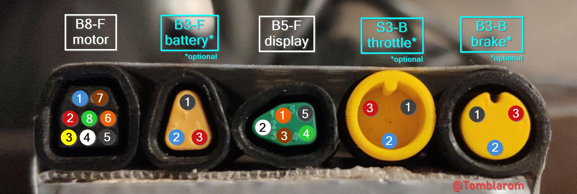
Here is the corrected wiring diagram. All pinouts: https://github.com/OpenSourceEBike/Bafang_M500_M600/tree/main/Hardware/Cables%20M500_M600


Attachments
Similar threads
- Replies
- 2
- Views
- 241
- Replies
- 5
- Views
- 2,873
- Replies
- 49
- Views
- 3,330
- Replies
- 65
- Views
- 7,684
- Replies
- 0
- Views
- 2,106