Futterama's power stage for Lebowski's controller IC

Some more scope shots. Lowering the gate resistor introduces a bit of turn-on ringing on the gate and drain-source and only gives a total turn off time improvement of about 90ns (from PIC output low to FET completely off = 1.184µs).

The gate is switched off pretty fast at 226ns, but the FET is really slow, it doesn't really start to switch off until the gate voltage is 0V and it takes the FET about 816ns to switch off - the FET datasheet has a value of 119ns "turn off time". Does the coil inductance have anything to say about the switch-off time?
 

Attachments

  • low_gate_resistor_ringing.png
    low_gate_resistor_ringing.png
    13.2 KB · Views: 2,754
  • turn_off_gate-source.png
    turn_off_gate-source.png
    15.2 KB · Views: 2,754
  • turn_off_drain-source.png
    turn_off_drain-source.png
    15.4 KB · Views: 2,754
Futterama said:
Does the coil inductance have anything to say about the switch-off time?
Well, a test answered my own question. Yes, it does.

3 scope shots:
Homemade high inductance, low current air coil = long turn off time: 816ns.
1:10 scale RC motor 6.5T, stator without magnetic rotor = short turn off time: 117ns.
1:5 scale RC motor "Beast", stator without magnetic rotor = short turn off time: 110ns.

I think I'll be testing with the RC motor stators from now on, they give better scope results :mrgreen:
 

Attachments

  • inductance_test_homemade_coil.png
    inductance_test_homemade_coil.png
    11.1 KB · Views: 2,750
  • inductance_test_1-5_RC_motor_stator.png
    inductance_test_1-5_RC_motor_stator.png
    11.3 KB · Views: 2,750
So, I got around to the high side FET. It's all connected according to the schematic here. The MCU pulses the low side FET T2 for 1ms to charge the bootstrap capacitor C1 through R5 (even though the bootstrap capacitor is actually already charged through the load), then a deadtime around 1µs and then a 1µs pulse to the high side FET T3. The scope probe is connected to the high side FET gate and the scope ground is connected to the high side FET source.

The scope shot don't look too good :roll:

Any advice?
 

Attachments

  • G-S_high_side.png
    G-S_high_side.png
    13.2 KB · Views: 2,718
  • gate-driver-sch2.png
    gate-driver-sch2.png
    3.3 KB · Views: 2,718
It's probably your layout, you have no ground plane to help shield from noise. Ground plane is connected to its respective high/low side source. Twisted pair connection should be ok to the power stage. You have a lot of ring in your scope shots.
 
If you are redoing the layout, your Buss should have the B+ and B- trace overlap each other as much as possible. This cancels out the magnetic field generated when the current flows. This minimizes the loop area which is important since it's a high di/dt area. This is the magnetic field that any stray parasitic inductance will pick up in your circuit. This is the reason when you run wires form the gate driver you twist them, same principal. If your traces are laid out on a PCB, one should be on top, usually the gate + and then below it is the ground plane that is tied to the source pin of the respective MOSFET group you are driving. Preventing the fields from ever happening is how you stop the other inductive pieces in your design from ever picking them up... if there is very little being radiated, then there is very little to be received. In reality, this is much harder to do than I just typed. I just did a rough draft of a new power stage and to get it's size down and still maintain full over lapping power rails (commonly referred to as a laminated buss), I had to design with a 4 layer board and use internal traces for the low current planes.
 
The layout I was referring to was the gate driver IC board which can be seen in some of my pictures (a long PCB with room for 3 drivers, only 1 is soldered/populated).

I don't know what you mean by bus B+ and B-. Are you referring to my FET layout?

With the new IC from TI, I would do as you are suggesting, route the trace for the FET gate close to the trace for the FET source. The traces will be really short since my FET's are not on PCB so I need twisted wires between gate driver PCB and FETs.
Out of curiosity I compared the trace inductance between side-by-side traces and PCB top-bottom traces using 1.6mm double sided PCB and 100mil trace width as base for the calculations. I used the online calculators. This really confused me, the results indicated that 2 closely spaced traces on the same PCB side would give lower inductance than 2 traces on each side of the PCB. I even tried to lower the PCB thickness to 1mm but still the side-by-side traces seemed better inductance wise.

Let's just say I route the traces on each side of a 2-layer PCB. Should all unused copper space be occupied by copper planes that are connected to GND? Or should I split it up so the planes close to the low side are connected to GND and the planes close to the high side are connected to the high side FET source?

I will start laying it out tonight and post my progress, that will probably be easier to comment on.

Edit: By the way, I can get 2-layer PCB, 35µm, FR4 in only 0.5mm thickness, that should be good for gate drivers so the distance between the opposing layers are even smaller which equals even smaller inductance :D
 
Futterama said:
Out of curiosity I compared the trace inductance between side-by-side traces and PCB top-bottom traces using 1.6mm double sided PCB and 100mil trace width as base for the calculations. I used the online calculators. This really confused me, the results indicated that 2 closely spaced traces on the same PCB side would give lower inductance than 2 traces on each side of the PCB. I even tried to lower the PCB thickness to 1mm but still the side-by-side traces seemed better inductance wise.
As far as I'm concerned that is still an "open point", did you see my comment on Leb's thread? http://endless-sphere.com/forums/viewtopic.php?f=30&t=36602&start=725#p848733
 
I kind of find it logical that traces next to each other is better than on the top / bottom of a PCB, just because in the latter
configuration you're limited to the PCB thickness, but OK

Who is your PCB manufacturer, Futterama ? I've had mine made by ViRus PCB, very happy with their service so far (I haven't actually
soldered yet so who knows, maybe the traces will separate from the PCB material). Just ordered the parts, hopefully will get them
on monday so I can start !
 
Njay, yeah, I did see your comment. The online calculators usually complains when the input does not meet the criterias.

Lebowski, 2 wide tracks next to each other, even if they are really close, can have larger center-to-center distance than 2 tracks on each side of the PCB. And isn't it the center distance that is important?

My PCB manufacturer is me. I use Presensitized Positive Photoresist PCBs. I have never had any manufacturer make any of my boards and I'm not going to anytime soon, I love making my own PCBs.
 
Futterama said:
Lebowski, 2 wide tracks next to each other, even if they are really close, can have larger center-to-center distance than 2 tracks on each side of the PCB. And isn't it the center distance that is important?

My PCB manufacturer is me. I use Presensitized Positive Photoresist PCBs. I have never had any manufacturer make any of my boards and I'm not going to anytime soon, I love making my own PCBs.
I don't know about the center to center distance being important. The whole clue about using a groundplane is that the return current of an opposite sided trace
flows directly underneath it through the groundplane, because this is the path of lowest impedance (read:inductance). Similarly, in two traces side by side I would
expect the current to take the path of lowest impedance, meaning it doesn't go through the middle but flows at the side of the trace closest to the neighboring trace. This
then implies the separation distance is important, not the center to center.

at the bottom of the page it shows a current density plot for two parallel (square) conductors carrying an equal but opposite current:
http://quickfield.com/advanced/hmagn2.htm
 
Futterrama,

Lebowski proposes an interesting theory and several of us are waiting to see what happens and if it works and at high power levels. The ground plane design is already proven to work to over 50kW continuous designs (directly, with twisted pair, or optical link, etc). Since you are just starting out you need to decide if you want to experiment or try to build based on known working concepts. There is nothing wrong with experimenting, but since I too am a beginner and only know the basics I chose to go with proven concepts so I can figure out the quirks of it first.

Getting a solid gate driver setup running well without lots of strange things happening such as overshoot/undershoot/preshoot/ringing/etc is difficult. It's very hard to believe such simple circuit diagrams can go completely crazy based on layout, especially since the frequencies they operate in are typically < 100khz... but the deceiving part is the how fast the rising / falling edge happens since it determines a lot of what goes wrong. Slowing down the rising/falling edge can help remove a lot of the mentioned issues.

This is one of those projects that requires you to build it and then spend time on the bench testing and tweaking it. I spent something like 9 months learning the theory and designing my setup and then about 2 weeks on the bench. That 2 weeks of bench testing made everything sooo much clearer, but I would not have been able to troubleshoot any problems seen on the bench without basic understanding of the theory.

It might be worthwhile to buy/build a working gate driver demo board so you have something to compare too. Several manufacturers offer them and they are usually < $150. You could also copy my layout (just the gate driver section) and build one of them for about $25, so far it's proving solid, but I have not run over 25A through it connected to a motor yet. I have done > 350A of a dead short and also shoot through into a single FET and the scope traces looked remarkably clean.
 
R1-R2: Gate resistors.
R3-R4: Gate-source resistors.
C1: Bootstrap capacitor.
C2: Bypass capacitor.

Red is top layer, blue is bottom layer. I haven't filled the whole bottom layer with GND plane yet so it is easier to see the blue gate return paths. The gate return path that is GND will be part of the whole bottom GND plane.

Looking better now? :D
 

Attachments

  • gate-driver-brd_new_for_TI.png
    gate-driver-brd_new_for_TI.png
    7.1 KB · Views: 2,670
I have updated my layout. I'm not sure if I need to force the return path for the low side gate on the blue bottom layer (from PAD8 to R1) or I should just let the polygon fill the area and the current will automatically follow the top trace since it's here the lowest inductance path is.
Lebowski, I think you have mentioned something about this before?
 

Attachments

  • gate-driver-brd_new_for_TI_bottom1.png
    gate-driver-brd_new_for_TI_bottom1.png
    5 KB · Views: 2,653
  • gate-driver-brd_new_for_TI_top1.png
    gate-driver-brd_new_for_TI_top1.png
    5.7 KB · Views: 2,653
looks like the traces overlap pretty well, I'm not sure about pad 8 and tying the top to the bottom as I haven't seen that done. Is this high/low combo driver or just one side? If it does both high and low sides you need 2 ground planes, one for the low side one for the high side underneath their respective components. I'd add a place for a G-S cap so you can adjust the on/off time with a small capacitor if it's too fast. I had this problem.

It would also be good to add an additional 10uF ceramic cap to the 15v supply rail with a 100nF bypass cap right next to it. The 10uF cap will supply high current peaks to the driver when required.
 
Zombiess, this is a bootstrapping, 4A peak, high frequency high-side and low-side driver (combo as you call it).

I don't quite understand what you mean by 2 ground planes. What do I connect these ground planes to? Low side ground plane should connect to GND/VSS/low side source right? Where do I connect the high side ground plane if not to GND/VSS/low side source? Should I connect it to high side source? And why? I have the high side source return path right below the gate current path, so the inductance is minimized by that.

Good point about a place for a G-S cap.

Additional 10µF? Like in one more than I already have with C2? Well, C2 is only 1µF and this is a calculated value. But now that I have a good scope, I can easily see if 1µF is not enough and it is pretty easy to replace. But I will take your advice and add a 100nF next to it (100nF closest to IC, then 1-10µF behind that or the other way around?).
 
Zombiess, I have been reading a bit on ground planes. I found a post where someone asked whether to poor copper on free space on the topside of a 2-layer PCB and then connect these to the bottom ground plane. All answers told him to poor copper and connect to the bottom ground plane.

http://www.edaboard.com/thread125695.html
 
Ok, so I think I understand why you want me to have 2 ground planes. And I don't see any other option than to connect the ground plane for the high side to the high side source.

My problem right now seems to be that I actually have the high side reversed regarding signal layer and ground layer - the gate connection runs on the same PCB layer as the ground plane for the low side (blue bottom layer) and the high side source connection is on the top PCB layer. I don't know if this is of any concern but it seems reverse of the layout techniques I know of (which basically is pretty limited).

My circuit is a bit alternative since the high side gate resistor is actually connected to the high side source. I saw this design in an app note from Fairchild regarding their gate drivers. They call this relocated and double purpose gate resistor. I have the option of connecting a diode between the high side source pin on the driver IC and GND. This should keep the negative voltage on the IC pin to a minimum, and the relocated gate resistor then acts as a current limit for this diode during the negative voltage transient of the source terminal.
I don't know if this is really necessary since: "The UCC27210/1’s switching node (HS pin) is able to handle -18 V maximum which allows the high-side channel to be protected from inherent negative voltages caused parasitic inductance and stray capacitance".
 
Futterama said:
zombiess said:
Good luck
Does that mean no more help from you? :shock:

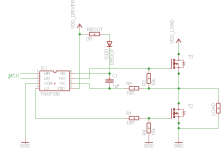
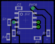
I can't help you with concepts I am unfamiliar with. Right now I know one method of design that has been proven to work. I am not knowledgeable enough to help beyond fundemental basics, and even that is pushing my skill level. I am still a noob to most of this and only have a single 90% proven design. I had a ton of help from highhopes but I understand what he taught me... well almost all of it. I got somewhat lucky by having my very first ever design work as planned. I am told 2 to 3 designs are usually required. I am of course most familiar with the td350e driver and have figured out most combo drivers are a pain to properly layout without doing a 4 layer board, but yours doesn't look so bad to layout. I can see why as i am now working on number 2 which is even better than what i posted, much smaller too. Laying out the board is the hardest part since its always going to be some compromise, but certain rules should be followed. If you download and steady the layout I did you can see how I did the ground planes for high and low side. Since you are paralleling the gets you should put a small gate resistor on each. The value should be about an order of magnitude lower than the main gate resistor.

Some suggestions.
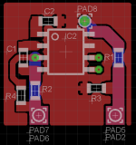
Make 2 ground planes, both on the bottom with a gap between them. One gets connected to high side source, the other to low side source.
Keep all components smd in the gate driver and placed on the top layer using as few bias and traces to the bottom side as possible. This takes many attempts usually, I spent several hours a day for a week due to how many components are in my driver.
Size your boot strap cap appropriately, there are online calculators but my guess is 6 to 10uF xr7 will be good.
Add a 10uF xr7 cap to the 15v rail, it should be very close to the driver, right after it use a 0.1uF bypass cap. Order should be power, 0.1uF, 10uF, driver ic. I skimmed the datasheet of your driver and they show this same configuration.

If fairchild offers a demo board for this chip, get the board layout or buy one. All the hard design work is done for you and you can borrow it :D

I went the hard route because I wanted to learn all the details and the math... I am a sick bastard like that, I don't accept just because usually always want to know why.

If I have some time... which I don't right now I will try to do a quick and dirty layout with your driver if so you can see some of the concepts. The other guys on here can then help tear apathy any mistakes I made.
 
Zombiess, when I'm working on this, I have a lot of questions. I ask those questions here and people tend to answer 25% of them, forgetting the rest. 50% of the rest comes to me, either by testing, searching Google, figuring out myself or something I read in other posts. The last 25%, well I'm lost and I guess I have to take those to another forum or something.
My point is really, the answers from you are some of those that give me a better opportunity to search for an answer or figure them out myself. So you DO know stuff and your help, and the help from others, are much appreciated.

Now, I guess you missed the post where I talk about a new driver IC I got from TI (Texas Instruments). The one from Fairchild is fine, but the propagation delay is 10 times the delay of the TI chip, and the TI chip has only slightly less drive current (4A for TI, 4.5A for Fairchild). The layout I'm doing here is for the TI chip (UCC27210/UCC27211). And I didn't find any evaluation board for the UCC2721X last time I had a look.

The only layout guidance I got from TI was page 16 in the datasheet. And the example component placement figure they put in there, seems to not follow all of the layout recommendations stated on the same page. So I'm trying, but it is hard when I don't know which rules I MUST follow, and which I can make a compromise with. An example I am struggling with, which is more important, wide traces (60-100 mils width as stated in the layout recommendations) or bootstrap cap close as possible to the IC.
 
New gate driver layout. Wirepads are without holes, power traces on each side of board to minimize inductance, same with gate traces, GND on top layer since one of the SOIC package options include an exposed thermal die pad. Probably need the big soldering tip to heat all that copper :lol:

C2, C6, C10 are soldered directly to the IC legs, quick and dirty way of getting a wide trace from pin 3 - well, the datasheet did say to place the capacitor as close to the IC as possible 8)

Next challenge is to develop this board using my single sided UV light box and still keep the 2 sides aligned :roll:
 

Attachments

  • gate-driver-brd_new_for_TI_ver4.png
    gate-driver-brd_new_for_TI_ver4.png
    12.7 KB · Views: 2,592
Doesn't look like you have separate high/low ground planes, just a low side. Since the high side is floating above ground you will probably end up getting noise.

Think of the single chip as 2 separate drivers. All the parts for the high side go over a ground plane referenced to the high side ground which is your phase output. The low side go over a second ground plane referenced to the gate driver ground.

I have my new layout virtually done. It uses 2 individual chips, but it has 2 ground planes on the same board... Well technically 4 since I am using isolated supplies and my input is opto coupled. I'll post up a picture of it. If you have kicad I can post the entire design if you want to look at it.

I know I saw some examples with split ground plane layouts for drivers like yours but I don't know where they are or what chip it was for. I abandoned that type of design months ago. Your driver looks much easier to do the layout on.

Can you fill out your location please? I would say use oshpark for the PCBs but I don't know what country you are in.
 
Back
Top