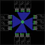
Futterama's power stage for Lebowski's controller IC

Location filled, I thought it was enough to put in my country, but that obviously didn't show up as I thought.

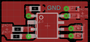
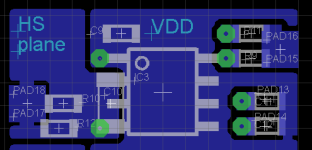
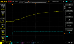
zombiess, R10 at pin 3 of the IC is the high side output gate drive, that's on the top layer where I also have my GND plane. Below R10, R12 and a part of the GND plane, I have the HS plane, HS is high side source. The HS plane is overlapping the GND plane, is that a bad idea? After you mentioned the noise issue, I can see that the HS plane should probably not be bigger than the high current path for the gate, on the top side.
 

Attachments

  • gate-driver-brd_new_for_TI_ver4_ex2.png
    gate-driver-brd_new_for_TI_ver4_ex2.png
    4.4 KB · Views: 2,603
  • gate-driver-brd_new_for_TI_ver4_ex1.png
    gate-driver-brd_new_for_TI_ver4_ex1.png
    4.3 KB · Views: 2,603
That is the concept I was talking about. The 2 ground planes should not overlap.

Are the green dots vias? If so it looks like you have a lot of them for so few components. Can you get all the components on the top?
 
Yes, the green are vias. I could probably get all the components on the top side, but the board would become larger and hence some of the gate traces would become longer.
What would it benefit to get all the components on the same layer? It would not decrease the number of required vias.

I would really only be able to eliminate 1 via, which I think I will, but only by putting C11 and C12 on the top side, and I will change those to SMD 0603 so it won't affect board size.

Regarding PCB manufacturing, I'm still very well capable of making them myself, it's part of the hobby for me. If I were to do 100 boards, then I would have them made, but for the few I need, I'm doing it myself. Vias will be 0.5mm drilled holes with a cutoff resistor lead put through.
 
Not sure I'm qualified to answer yet. I'm still struggling to minimize the gate loop area on my new power stage layout and failing :(
 
Futterama said:
I was wondering if I could use SMD 0603 gate resistors. But can they handle the 4A peak current?

I don't think I'd tempt doing that. I use 2512 size for all my gate resistors. My 0.5 ohm gate resistors are 1210/1206 sized. This way I don't have to worry about heat causing issues. It's probably best to oversize them, I don't think I'd personally go smaller than 1206.

If you can wait on making your PCBs for a week or so I'm trying to start a new thread with the help of HighHopes on how I kept failing at designing my power stage gate input parts. I want to show all the failed ideas and what was wrong with each one until I finally got one that looks like it's going to be OK.
 
zombiess, the size of my gate drive resistors are 0805 right now. 0805 have a typical power rating of 0.125W.

Let's assume I would be running max 32kHz PWM. That is 64000 current pulses back and forth through the gate resistor (charge and discharge the FET gate).
Assuming charging/discharging the gate in 500ns. Then the resistor will see current for 32ms every second. If the gate current was a constant 4A (as this is what my drivers can deliver), the resistor would see an average of 128mA. That's almost 2W at 15V. But the gate current is not 4A through the whole charge/discharge of the gate. I don't know how to calculate the total current going through the resistor during a charge or discharge, but I do know it is much less that the 4A peak.

I think I will do an experiment :D

Yes, I can surely wait a week, as you can see, I have an experiment to do and I also have to get the thin 0.5mm double sided PCB ordered and delivered first. It will be interesting reading, I'm looking forward to read it.
 
Futterama said:
I don't know how to calculate the total current going through the resistor during a charge or discharge, but I do know it is much less that the 4A peak.

I can save you some time, I have all the formulas in a spreadsheet. It's not really ready for prime time use, but the first tab titled Driver Current should get you started.

Just fill out the green section with you info and the blue sections will be calculated for you. Orange is the math formula being used. This sheet is devoted to sizing the gate drive power supply and calculating how much wattage is passing through the gate resistors so you can size them properly. There are notes as to what each section on the sheet is calculating and I currently have it filled out with data for 2 parallel IRFP4568 MOSFETs. It's setup for 16khz PWM with an 8 ohm gate resistor with a 15V Vgs voltage. The section you are interested in is towards the bottom if you are only using one resistor vs separate on / off resistors is the

IrIrms_TOTAL = square_root(Irms_On^2 + Irms_OFF^2)

and

PRgTOTAL = Irms_TOTAL^2*RgON

If you plug in your data it should tell you what your gate drive current and mW through the gate resistors will be so that you can size them as required. In the example in my sheet I need a minimum of a 250mW resistor, so that means I should run a 500mW resistor so there is overhead. You are at the entrance of the rabbit hole, it goes deep. I still haven't found the bottom but I think I might see it. If you check out some of the comments on the notes page (you'll have to expand some rows to see all of them) it will give you a good idea of what's involved. That's where I got the formulas, from a working example. All of this needs to be taken into consideration to do it right.

I also have sections on sizing the boot strap capacitor and DC Link capacitors. The desaturation and 2 step turn off don't apply since your gate driver doesn't used them.

I hope this helps you. When I was starting out I saw a lot of these but they were scatter in lots of different app notes. Until I had someone teaching me design method I wasn't able to put it all together. Gate driver design looks deceptively simple. My first design took me 9 months and that was with someone teaching me!
 

Attachments

  • Driver Calcuations IRFP4568.zip
    107.2 KB · Views: 54
zombiess, thanks for the datasheet. I think there is an error somewhere because when I set the Rg_ON and Rg_OFF to the same value (4 ohms) the tpON and tpOFF is the same but the IpON and the IpOFF is not the same, actually the IpON is 3.45A and the IpOFF is 0.3A. The V_Off is set to 0V, but shouldn't this value be the voltage the gate is charged to before turning off?

Anyway, when I set V_Off to 15V and Vg to 0 volts (I have no push-pull transistors), the sheet calculates the power dissipated in a single resistor to 273,9mW.
Lebowski's calculation gives me 51mW.

I'll do my test, and pick a size resistor that does not burn my finger at max gate drive current (4A) at max expected frequency (32kHz) using max number of parallel FETs.
 
Lebowski said:
for the dissipation in the gate drive resistor, it's easiest just to take:

P_res = Q_gate * V_gate_drive * F_pwm

if I remember correctly

Isn't it best to convert to RMS since we are dealing with large peaks?
 
zombiess said:
Lebowski said:
for the dissipation in the gate drive resistor, it's easiest just to take:

P_res = Q_gate * V_gate_drive * F_pwm

if I remember correctly

Isn't it best to convert to RMS since we are dealing with large peaks?
It's an equation that gives the power directly, so no need to convert to RMS. You only need to convert to RMS if you use I_rms^2 * R or V_rms^2 / R.
 
Lebowski said:
zombiess said:
Lebowski said:
for the dissipation in the gate drive resistor, it's easiest just to take:

P_res = Q_gate * V_gate_drive * F_pwm

if I remember correctly

Isn't it best to convert to RMS since we are dealing with large peaks?
It's an equation that gives the power directly, so no need to convert to RMS. You only need to convert to RMS if you use I_rms^2 * R or V_rms^2 / R.

I just looked through my notes and I recognize that formula as a combination of the 2 I have for for calculating the gate drive power supply requirements.
Idrive = Qg * fsw - Average Current supplied to the gate driver.
Pg = Idrive * delta_Vdr - Average gate driver power supply wattage required.

It can be short cut into Idrive = Qg * fsw * delta_vdr which is the same as your P_res = Q_gate * V_gate_drive * F_pwm formula.

The gate drive pulses tend to be more triangular / trapezoidal so I believe RMS is a better method.

I have the following notes on these two different yet related topics as this:

drive = Qg * fsw - Average Current supplied to the gate driver.
Pg = Idrive * delta_Vdr - Average gate driver power supply wattage required.
NOTE: This is the average current essentially between the power supply and the gate drive IC's decoupling capacitor. The average drive current used for power dimensioning of the power supply only. The RMS current between gate drive IC and MOSFET is used for dimensioning gate resistance because when current goes into gate it is basically triangularly shaped, and for power we need to do the calculation in RMS, so you need formula for repetitive triangular pulses.
 
I couldn't wait any longer for my order of 0.5mm double sided PCB and various valued 1206 resistors to show up, so I made a PCB using normal 1.6mm double sided PCB material and my new gate drive IC and new PCB layout. I used a 0R gate resistor and left the 4R7 through hole resistor at the gate pin of the FET in my test setup.

I still see a lot of ringing at the FET gate leg. I will try with a 10R gate resistor and I will also add an extra bypass capacitor to the IC, I have 660mV p-p ringing at the IC supply when switching ON.

The good news is the propagation delay compared to the other gate drive IC. The "old" gate drive IC measured to around 120ns delay, the new IC measured to around 40ns.

I have two scope shots for you. One measured at the FET gate and source legs. The other is measured at the PCB where the twisted wires are attached. There is also a picture of the setup, and yes, I know the probe is connected at the PCB and the ground clip is connected at the FET source, don't mind that :lol:

Any thoughts and suggestions are welcome :wink:
 

Attachments

  • G-S_at_FET_leg.png
    G-S_at_FET_leg.png
    12.1 KB · Views: 2,436
  • G-S_at_PCB_where_wire_is_attached.png
    G-S_at_PCB_where_wire_is_attached.png
    11.6 KB · Views: 2,436
  • 20140315_152202_Android.jpg
    20140315_152202_Android.jpg
    210.2 KB · Views: 2,436
My recent order arrived so I now have more SMD gate resistors to test with but haven't had the time to do the actual tests. I have been thinking about my FET and busbar arrangement and came up with a new idea.

This is just a quick illustration. It is 4 pairs of individual 6-FETs, where only the 3 lowside FETs of the 6-FETs are shown. So no parallel FETs, just parallel 6-FET sections just like Lebowski recommends so the current is divided into 4, giving lower current through each busbar.

It is the same idea as with my SMD FET layout, but that design is taking too much of my design time and still I'm not 100% sure I will be able to assemble/solder it and it is going to be a pain to replace a single blown FET, so I'm thinking of a TO-220 design like the one on the pictures. I am also thinking of laminate busbar with 0.2mm copper foil, but the busbar is so short in this design, I don't think it would be worth the extra hassle. Maybe I'll just use the 0.6mm copper plates like Lebowski, and do a laminate busbar with those, actually just to increase the busbar thinkness so the FET legs fit better. More info and pictures to come when I have had some more time to work on the idea. As far as I understand from Lebowski, the important thing is to keep the inductance between the individual FETs low, and also between the FETs and the bypass capacitor. Inductance between the individual 6-FETs is not so critical and a higher value can even be beneficial for protecting the 6-FETs from each other.

Too many non-hobby stuff is going on in my life right now :? but I hope I will find some time to do some more work soon.
 

Attachments

  • new_idea.png
    new_idea.png
    5.9 KB · Views: 2,319
A few scope shots of my gate driver. The gate resistor is 20 ohm. I used my little probe spring for the ground connection, they do help a lot on the waveforms.

Gate-source waveforms, looking pretty good. I need to make a new board using the thinner PCB and I will try to include the Lebowski-style turn-off diode for lower gate off resistance.
 

Attachments

  • DS1Z_QucikPrint4.png
    DS1Z_QucikPrint4.png
    13.5 KB · Views: 2,247
  • DS1Z_QucikPrint5.png
    DS1Z_QucikPrint5.png
    11.6 KB · Views: 2,247
Source-Drain scope shot. The blue trace is the input to the gate driver IC. It takes forever to turn off the MOSFET due to the single gate resistor configuration and also these particular MOSFETs is for testing only, they are old and deprecated and have a total gate charge of 200nC typ, 300nC max.
 

Attachments

  • DS1Z_QucikPrint1.png
    DS1Z_QucikPrint1.png
    13.4 KB · Views: 2,244
The current in the coil is probably relative small due to the short pulse (only a few µs). So I did some tests with a longer pulse, here is the turn-off shot of a 150µs pulse.

View attachment 1
Somewhere between 150µs and 200µs pulse length, an interesting thing happens. The waveform looks very different after turn-off. My guess is that the local 1000µF capacitor runs out of charge :lol:

DS1Z_QucikPrint6.png
 
I'm trying to calculate the average current of a turn-off diode (the diode used to bypass one of the gate resistors at turn-off) and I'm not 100% sure I got it right, my result is way lower than expected (or rather feared).

I'll calculate using extreme values. 30kHz and 1.5A peak gate current. I'll probably never go as high as 30kHz switching frequency, and the 1.5A is peak but I'll calculate it as average just to put in a good safety margin.

I'll assume a turn-off time of 1µs, again a big number with a good safety margin.
So, 30k turn-offs each second, lasting 1µs, gives a total of 30ms. So the diode will carry current for 30ms each second. Assuming the current to be the 1.5A, gives 1.5A*0.03s = 0.045A.

Is this totally wrong?

I'll use the average current to calculate the power dissipation in the diode, just so I don't pick a too small diode. But with around 500mV forward voltage and average current of 45mA, the dissipation is really low at ~23mW.
 
I am not shire about the turn off current value as its not something I have seen discussed before. In my new gate driver layout with a 15a boost stage I am using a schotky diode in series with my turn off resistor. It let's me turn off the MOSFET faster than I turn it on. I am puzzled as to why your current turn off is so slow. It should be about the same as your turn on unless the MOSFET you are using has a really slow fall time. Have you tried a different MOSFET? Maybe something common like an irfb4110 if you have one laying around.

BTW, what is your target amps? I have my setup running now and am pushing 200a phase with a 24 MOSFET setup. Max MOSFET case temp is 60c so far and I had to beat on it hard just to get to 60c and I was at 225a, 25a past the sensors rating (but I checked them on the bench, this is the abs max they will measure). I have a lot of aluminum and surface area.
 
zombiess, I have not tried another MOSFET yet but I do have some of the new CSD1953KCS from TI to try out. I don't have any IRF devices to try. The MOSFET I'm using now does actually have a faster turn-off time than turn-on. I have attached some numbers from the datasheet.

Target amps is 200A peak for a few seconds, that's the max my motor will use. I'm working on a low inductance output stage, Lebowski style, to attach the MOSFETs directly to my PC cooler heatsink. I have room for 4 x 6-FETs so I will end up with 24 FETs like yours.
 

Attachments

  • Capture.PNG
    Capture.PNG
    32.9 KB · Views: 2,159
zombiess said:
I am puzzled as to why your current turn off is so slow.
Well, it actually makes good sense to me when looking at the gate-source shots. The MOSFETs gate-source threshold is around 2.3V. It does not take as long to charge the gate from 0V to the threshold of 2.3V, as it takes to discharge the gate from the 12V down to the threshold.
 
With a threshold that low I would be running - turn off!
 
Back
Top