Futterama's power stage for Lebowski's controller IC

Futterama said:
Flux pen and solder? How would you arrange that?

I'm thinking reflow solder paste in a syringe but I haven't got one yet as the shelf life is only a year.
Oh sorry. I used the solder paste. I would not worry about the year self life. If you buy the right amount its no big deal. And you can keep it sealed and cool to make it last longer.
 
Futterama said:
Arlo1 said:
I would not worry about the year self life. If you buy the right amount its no big deal. And you can keep it sealed and cool to make it last longer.
So what it the right amount?

I know to keep it cool, like in the fridge.
Just order some and see how long it lasts. I ordered a 10 oz syringe and I think its enough for a year for me but that totally depends on how much of this I do things might change in a month or two if my build works out I will be building a few for others as well.
 
I finished my hot plate and have already used it several times to replace the LT3999 on the modified demo board, I keep damaging them for some reason. Well, I did make a mistake on the PCB for the bigger transformers, maybe this damaged the LT3999 switches. Anyway, I just tested the second biggest transformer, and it seems to work better than the smaller ones. I think it has something to do with the copper losses in the transformers, it will be higher in the smaller transformers due to the smaller wire size, so the bigger transformer is better at keeping a higher output voltage vs. the input voltage.

Here is my hot plate:
 

Attachments

  • hotplate.jpg
    hotplate.jpg
    60.8 KB · Views: 3,075
So, I have been doing some more tests with the LT3999. I used MBR0530 (0.5A schottky diode) as output rectifiers and I found one that failed cause I got strange readings on the output. So I replaced the faulty one and things were good again. But my output power was limited, and without fan cooling on the PCBs, the output voltage would suddenly drop after a while. I thought the LT3999 was activating it's overtemperature protection, but it didn't seem very hot, but the output rectifiers was a bit hot. So I replaced the output rectifiers with FMKA130L (1A schottky diode) and things were much better now. The output voltages are closer matched and I don't experience the same 9-10W output limit.
I have also tried using one of the biggest transformers, the one with the highest current rating, but compared the to second biggest transformer, I don't see much improvement regarding effeciency and no improvement on output voltage variations when running at 10W output. Maybe this will change when I start adjusting/lowering the switching frequency to improve the effeciency of the LT3999 switches. Right now, I have the highest current rated transformer connected, giving 12W output with 75% effeciency at 18V input without fan cooling. The hottest component is the LT3999 so next step is to lower the switching frequency to gain some effeciency in the LT3999 and keep the temperature down.

I don't need more than 15V output, so the 12W output is just a test to see if the circuit can handle this kind of output power. As of now, I have no real numbers on the required power for my gate drivers, but I would like to find the limits of my components so I have a number for the limit of this kind of gate driver supply.

Latest numbers with 12W output (disregard the actual output voltages, I just found it easier to raise the voltage than to replace the load resistors):

Input
18,04V @ 895mA = 16,15W

Output
16,67V @ 46,3Ω = 6,00W
16,92V @ 139,7Ω = 2,05W
16,77V @ 139,6Ω = 2,01W
16,87V @ 139,5Ω = 2,04W
Total output: 12,11W
Effeciency: 74,98%
 
LT3999 running at 600kHz, Würth 749196301 transformer, FMKA130L rectifiers.
16.65V input at 910mA = 15.15W.
4 x 15V output (15.12 to 15.51V depending on output).
Total output: 12.29W.
Effeciency: 81%.

Output voltage ripple is dependant on the output capacitor, it will have to supply the load in the off-period which is 833ns at 600kHz. With 4.7µF, the ripple voltage is well below 50mV.

The output voltage variations between the different outputs can be a result of my load resistor setup which consists of a handful of different size and value resistors since I don't have 112.5Ω and 37.5Ω power resistors around. It can also be a result of transformer winding differences, I'll look more into that.

The best news is really that the LT3999 and the output rectifiers are running cooler at the lower switching frequency, so I'll try to remove the heatsink in a minute, right now the circuit is powered and running so I can see it's stable.

The transformer used is the second biggest from Würth, it measures around 18x18mm and is 8.3mm in height. I'll say this is a quite compact isolated gate driver supply considering the output power capability 8)
 
A quick change, putting the capacitors on the PCB instead of on the breadboard, fixed the issue regarding wide output voltage variation, the output voltages are now within 150mV of each other.

I have removed the heatsink from the small LT3999 demoboard and starting low at 10V output voltage, which will reduce the output power since I use the same load resistors. So I'll keep an eye on the LT3999 temperature as I raise the voltage to see if I will hit a thermal limit before reaching 15V/12W output.
 
No thermal limit up to 15V output (I haven't tried higher than 15V). PCB will get hot, around 75°C measured with my Fluke probe with a dab of white thermal grease, near the LT3999 on the PCB backside. Effeciency takes a small hit with higher temperatures, probably from the higher switch resistance in the LT3999. At 75°C, effeciency is 1% lower than when I point a fan at the PCB and temperature is down at 35°C.

The LT3999 devices I got are the wide temperature range type, LT3999MP. From the datasheet:
The LT3999MP is 100% tested and guaranteed over the –55°C to 150°C junction temperature range. High junction temperatures degrade operating lifetimes; operating lifetime is derated for junction temperatures greater than 125°C.
So a PCB temperature of 75°C is not alarming. The PCB is small, with a bigger PCB, the thermal performance will be better, so I'm not worried.
Also from the datasheet:
At a junction temperature above the operating temperature range the thermal shutdown function turns off both switches.

I'm pretty sure the LT3999 devices that failed on me, was due to the failure in the output rectifiers, and somehow this has generated spikes back to kill the LT3999 switches, and hence had nothing to do with LT3999 junction temperature. Since I changed output rectifiers, I have not had a LT3999 failure.
 
Good, you're doing great :)
DC-DC converters is also a fascinating subject. You should build yourself a basic dummy load (constant current sink), it's very simple and yet extremelly useful for several things. I've built something like this exactly for some DC-DC converters tests, with components I had laying around:

varload.png


"FEM" is the device under test, I have a schottky in series with the FEM+ line for reverse polarity protection and the 1K pot is for fine adjustment. If you're using up to 1A or so you can probably skip the 2N3055 and have it work at "high current" to a bit lower voltage. You can also use a TL431 instead of the zener if you want better precision/stability. There's tonnes such schematics around.
 
Njay, thanks, and thanks for the schematic, but I currently have the resistors matched to 0.15% so I think I'll keep them as they are, soon the load will be a gate driver anyway :D

I have one last problem to solve with the LT3999. Sometimes it does some wierd stuff on the switches (see the scope shots), I have asked the Linear FAE about this and is awaiting answer.
It does this when I connect the circuit to my powersupply using the banana plugs. It only happens if the power supply is turned on and set to more than about 14-15V, and all the load resistors are connected. If I connect the circuit to the powersupply and then turn the powersupply on, it doesn't happen.
Also when it happens, I can fix it by disconnecting one of the load resistors, and connecting it again - it turns back to normal when the load resistor is reconnected :?
I have tried various things like extend the soft start period, adding more input capacitance ect. Maybe I have messed something up on the demo board, I have soldered and desoldered components many times now (e.g. when changing switch frequency) so maybe that has something to do with it, as I only first discovered this problem yesterday.

When looking at the scope shots, it could look like the internal current limit kicks in about 400ns after the switch has turned on, and resetting again after about 75ns. Maybe the transformer saturates (due to suddenly applied full voltage, 16.5V instead of e.g. 13V??? :shock: ) even though I'm nowhere near the µVs limit of the transformer with this switching frequency.
Typing this kind of thing down, explaining the problem, just gave me some more things to try out while waiting for my FAE to reply :D

EDIT: Well, it can't be the current limit kicking in because, from the datasheet:
When the current limit is reached the switch is immediately turned off and remains off for the remainder of the cycle.
As seen on the scope shots, the switch does not remain off the rest of the cycle.
 

Attachments

  • switch_weird.png
    switch_weird.png
    13 KB · Views: 2,995
I got myself a cheap USB microscope for christmas. It's for solder inspection after soldering the small things like the LT3999. I was not satisfied with the zoom level, see the first picture. So I chopped it up and made it shorter so now I got a very nice zoom level. I can even see the individual toner particles on my PCB toner prints :D

The microscope is this one: http://eud.dx.com/product/portable-10x-800x-usb-digital-microscope-w-8-led-844249254#.VK6qjiuG8mM

The stand is a flimsy plastic stand, so I attached a 4mm stainless steel plate on the bottom using VHB tape, to keep the base flat and to add some rigidity in the form of weight.
When zooming way in, every time I adjust the focus (on the grey thumb thingy), the microscope moves because of the plastic stand so it is really hard to get a good picture. So I have 2 more modifications in mind.
The first is an electric adjustment of the focus using a small RC servo. This way I won't have to touch the microscope to adjust focus and it won't move during focus adjustment.
The second is a metal stand for better rigidity, but this may not be necessary if my servo focus system turns out as expected.
 

Attachments

  • 1.jpg
    1.jpg
    76.6 KB · Views: 2,923
  • microscope.jpg
    microscope.jpg
    56.7 KB · Views: 2,923
  • 1501081657492562394.jpg
    1501081657492562394.jpg
    69.5 KB · Views: 2,923
  • 150108162915848411.jpg
    150108162915848411.jpg
    93.5 KB · Views: 2,923
I love it. I will be getting one.... Thanks for the link. I am so thankful for DX.
 
Arlo1 said:
I love it. I will be getting one.... Thanks for the link. I am so thankful for DX.
I should mention that if I had the choice of ordering myself, I would have gotten this one:

http://eud.dx.com/product/usb-powered-200x-300kp-8-led-aluminum-alloy-electron-microscope-w-holder-silver-844309040#.VK7hCiuG8mM

It is of brand "Andonstar". I even still consider to get this one, but the modding of the one I have is too much fun right now :D

Here is a review of both types: https://www.youtube.com/watch?v=H2P1_JZYnVc
 
Right now I'm using it to find the best solution for printing an Eagle board layout on my HP LaserJet 1018 printer. There are small differences in how the printer will print the ultra small DFN10 footprint.
Example: I have read that for some reason, it helps to round the edges of the pin footprint towards the thermal pad in the middle to avoid solder shorts under the part. So I edited the package in my Eagle library to include a rounded edge. The result is seen in the first picture, the dot of wire I added to the square SMD pad is slightly offset to the right.
In the second picture I just route a piece of wire towards the thermal pad before routing away from the IC.

Last time I printed a DFN10, the pads looked better when I rotated the layout 90°, so it seems the printer has it's limits - it is an older model with only 600 x 600 dpi but this type of model has a short paper path that doesn't wrinkle my special milky paper for PCB manufacture.
 

Attachments

  • rounded_in_package.jpg
    rounded_in_package.jpg
    55.6 KB · Views: 2,903
I just did a quick PCB fab from some two sided presensitized PCB material, I wasn't sure of the result since the PCB material was getting old but it turned out OK. Look at those beefy toner traces on the paper, and then look at those skinny traces on the PCB. This is probably due to the PCB being old, and was probably not 100% developed so I had to leave it in the etch tank for longer and the etchant eats its way in under the copper protection layer. Look at the last picture, you can even see the etch contours in the copper :shock:

Oh, by the way, my microscope focus is now controlled by a small RC servo :D so it's easier to focus in small steps 8)
 

Attachments

  • 15011023401118356388.jpg
    15011023401118356388.jpg
    51.7 KB · Views: 2,888
  • 15011023275917624774.jpg
    15011023275917624774.jpg
    88.8 KB · Views: 2,888
  • 15011023323217897433.jpg
    15011023323217897433.jpg
    62.4 KB · Views: 2,886
  • 15011023593719522464.jpg
    15011023593719522464.jpg
    68.5 KB · Views: 2,886
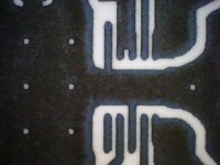
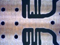
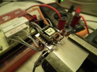
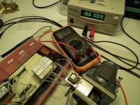
Time for a small update. I made a new PCB again, this time from some never presensitized PCB material which gave better results. I also tested my tin plating solution which I bought a while ago, works great.

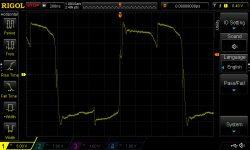
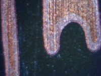
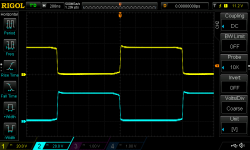
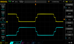
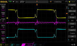
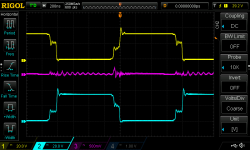
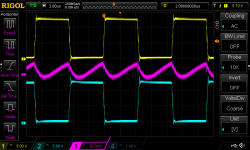
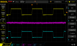
Anyway, I'm into the RC snubber business now. The switch nodes experience heavy ringing and this causes anormalities in the LT3999. So I need to add a snubber to the switch nodes. One way is to add 1 snubber connected to each switch node. The other way is to add 1 snubber from each node to GND. I get different results, and need to figure out the best way to do it. The snubbers I have tried so far, can give awesome results but will raise the input current with 100mA which is way too much.
The snubbers give different results when I connect the outputs in different configurations. I also found that the output diodes play a big role on the ringing. The FMKA130L diodes I switched to, must be kinda slow to reverse recover (no data about this in the datasheet), because I tried switching to S320 diodes which does have reverse recovery data in the datasheet (14-30ns) and this removed a lot of the switching abnormalities under certain conditions.

So where does this leave me now? Well, I know the output configuration and snubber configuration is somehow connected, this is good because I will be using another output configuration for the brain power.
I know I need to get hold of some snubber capacitors (ceramic C0G types perhaps?) and snubber resistors (broader range of values than I got now) to be able to get this right.
I will redesign my board once again and try to further reduce the stray inductance between LT3999 and the transformer. I have ideas for 2 different layouts and will be testing both of them.

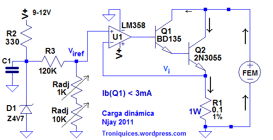
I got my information about how to calculate RC snubber values from these links:

http://www.maximintegrated.com/en/app-notes/index.mvp/id/3835
http://www.ti.com/ww/en/analog/power_management/snubber_circuit_design.html
http://www.digikey.com/en/articles/techzone/2014/aug/resistor-capacitor-rc-snubber-design-for-power-switches

Of course the different sources have to make life hard for me and raise further questions:
- Use film or ceramic C0G capacitors for the snubber?
- In the calculation of the parasitic inductance, use the stray capacitance AND the added capacitance or only the stray capacitance?

Any help on the snubber calculation from zombiess or HighHopes perhaps? :D
 
I just found this document and did some calculations from it:

http://www.nxp.com/documents/application_note/AN11160.pdf

[strike]Unfortunately the sanity check, the last part of chapter 3, does not work with my values. So I looked for the appnote directly on NXP's website, but couldn't find it with the search tool, so perhaps it has been discontinued due to this error.[/strike]

The idea of adding a single capacitor and calculate from there was more appealing than to solder and desolder a whole range of capacitors to find the one that would cut the ringing frequency in half.

EDIT: I made a mistake in my spreadsheet so the sanity check does work! I just digged further in the formulas and realized the sanity check actually gave the right value but the calculation for parasitic inductance had an error.

Now, they still disagree on the snubber capacitor value for critical damping. The NXP appnote above uses a calculation, the TI paper uses a thumb rule. The results are nowhere near each other :?
 
Futterama said:
Now, they still disagree on the snubber capacitor value for critical damping. The NXP appnote above uses a calculation, the TI paper uses a thumb rule. The results are nowhere near each other :?
Cool, space to innovate :)
 
The calculated snubber values from the NXP and TI documents using a damping of ζ = 1 is much better than using the Maxim document which uses a damping of ζ = 0.5.

Right now I use 2 snubbers, one on each switch node. The resistor should apparently be the one that connects to GND, from what I have read. The value is 20Ω, it was calculated to 24.6Ω but 20 seems to be a bit better. The capacitor was calculated to no less than 291pF but a 1nF seems to do the job, but this does increase power dissipation but not to unacceptable levels.

The result is very nice looking waveforms on the switching nodes, even under load, with minimal overshoot and no undershoot, which is important since the LT3999 can only handle down to -0.3V on the SWx pins.

12W single output is possible even with the high forward voltage of the S320 diodes (0.9V each).

Moving on with 4 outputs and tweaking the snubber values to optimize power dissipation. Also I'm working on a revision 6 of the PCB where I might put the transformer on the opposite side of the PCB so I can get the LT3999 even closer to the transformer pins to reduce inductance and capacitance.
 

Attachments

  • 17V 90mA 20ohm 1nF no load uden dioder SWA-SWB.png
    17V 90mA 20ohm 1nF no load uden dioder SWA-SWB.png
    13.6 KB · Views: 2,720
  • 17V 940mA 20ohm 1nF 15ohm load med dioder SWA-SWB.png
    17V 940mA 20ohm 1nF 15ohm load med dioder SWA-SWB.png
    14.3 KB · Views: 2,720
  • 12W rectified load with output ripple.png
    12W rectified load with output ripple.png
    19.5 KB · Views: 2,720
More update. New PCB with LT3999 and transformer placed closer together gave 80nH instead of 140nH. Pretty neat. Lowered the snubber resistor to 8.2Ω which allows me to use 470pF capacitors and this reduces snubber dissipation. Changed output diodes to SK24 which has lower forward voltage. Quick test showed more than 13W usable output power at 15V after bridge rectifiers :D
 

Attachments

  • DS1Z_QucikPrint8.png
    DS1Z_QucikPrint8.png
    17.2 KB · Views: 2,674
More test of the new setup, this time without bridge rectified output, but single rectifier on each output according to my 2W:2W:2W:6W output topology. This means that one of the switching nodes of the LT3999 will supply power to the 3x2W outputs, and the other switching node will supply power to the 6W output.

The waveforms on the switching nodes looks clean with no excessive ringing, overshoot or undershoot. The ~10V overshoot is acceptable since the LT3999 can take up to 60V on the switching nodes. A higher value RC snubber capacitor will bring this overshoot down, but will also increase snubber power dissipation.
The SK24 schottky diodes really does a lot better job than all the 3 types I tried from Fairchild Semi. The LT3999 switching frequency is 619kHz (RT = 22kΩ) and I think I will keep it here, maybe play around with it a little and have a look at the efficiency. Going too low will violate the µVs product of the transformer, going higher will increase LT3999 switching losses and probably also the losses in the output rectifiers.

So now I finally reached my final goal which was 12W total output without glitches :D

The efficiency is also better than ever, the PCB is small and does not get as hot as it used to, no heatsink anymore :mrgreen:
By the way, I'm back at using the MSOP devices and not the DFN device, the MSOP is just easier to hand solder.
 

Attachments

  • DSCF3676.jpg
    DSCF3676.jpg
    64.8 KB · Views: 2,652
  • DSCF3675.jpg
    DSCF3675.jpg
    92.3 KB · Views: 2,652
  • Output_power.png
    Output_power.png
    4.9 KB · Views: 2,652
So now I'm started on the switching regulators that regulates the input battery voltage (8S-12S LiPo, 24-50V) down to something useful. Right now I'm working with the LT8620 which takes up to 65V input and can output up to 2A. I want 3 of them, one for the isolated gate driver supplies, one for the isolated MCU supply and one for cooling fan output because they have each their voltage needs. I'm using the same part for all 3 voltages even though the current needs are different, because it's just easier to make 1 design than 3 different designs. I'll be syncing their clocks, probably with a LTC6902 multiphase oscillator, just to avoid any possible problems due to slightly different switching frequencies on the three LT8620, as recommended by the Linear Tech FAE.

I'll have to wait for some components to arrive for the LT8620 design, so while waiting, I'm working on the isolated MCU supply. I wanted to try out the LT3439 which has slew rate controlled switches for ultralow noise. I did a quick singlesided PCB, using some of the things I learned from my work with the LT3999. I used a Würth 749196201 transformer which has a current rating at almost 1A and a high µVs rating compared to the other smaller transformers from Würth - I need this since the LT3439 cannot switch faster than 125kHz, my setup was at 114kHz. I tried adding the optional LC filter on the output and it works like a charm, look at those scope shots :D That's less than 10mV ripple/noise at 320mA output at 5.5V 8)

Since the LT3439 push-pull topology is unregulated, I will add a LDO on the output so the Lebowski chip will get rock stable low noise voltage. I have my eyes on either the LT1764A or the LT3022. 1A output will be plenty and I like the low dropout voltage of the LT3022, but the LT1764A has lower noise and faster transient response. Also, during my test with 320mA output at 5.5V, the voltage will raise to 8V at no load. So maybe I'll be getting close to the max 10V input of the LT3022, so the LT1764A is probably the better choice.
 

Attachments

  • Output noise without LC filter.png
    Output noise without LC filter.png
    22.3 KB · Views: 2,619
  • Output noise with LC filter.png
    Output noise with LC filter.png
    17.5 KB · Views: 2,619
Why don't you just daisy-chain a couple small 24Vdc fans together and connect them to your batteries? the'll work great without any circuitry at those votages (you could also do 3 or4 12V). (edited due to math dislexia)
You could add a thermostat inline to control it if needed.
 
Back
Top