Seeking Help: BLDC Motor Control Board Development (FOC Technique)

Hello everyone,

I’ve been trying to understand this concept for quite some time, but I’m still a bit confused — I’d really appreciate any insights you can share.

How does an op-amp measure negative current when using low-side current sensing?
I’ve done a lot of reading and research, but I’m still not entirely sure how it works in practice.

Specifically, I’m trying to understand:
  • In what situations does the low-side MOSFET conduct current [how opamp measure negative current?]?
  • When and how does the body diode conduct current back to the phase or to upper MOSFET body diode through body diode?
  • How is this reflected as negative current in the sense resistor and measured by the op-amp?
If anyone could help clarify this or point me to a good resource — like an article, application note, or video — that would be really helpful for my understanding. I’d be very grateful!

Thanks in advance!
BldcLover
The current though the motor is pseudo continuous. It changes slowly because of inductance.

The mos are sequentially conducting high side then low side, swapping very fast relative to the current change

So whether the current is flowing in or out of the motor, it will still be conducting through the low side shunt when the low side FET is conducting.

Hence you can measure it. You just bias the opamp so that 0A is mid rail... 1.65V usually.

It's that simple.
Hi mxlemming,

Apologies for the delayed response — I’ve been feeling unwell recently, which led to a slight delay in my work.

In the meantime, I’ve been studying more, and based on my understanding, due to MOSFET switching, the motor doesn’t accept an instant change in current. As a result, reverse current may flow from ground to the motor phase — is that correct?
I’ve attached an image to illustrate what I mean; could you please let me know if my understanding is accurate?

I’m particularly confused about how the low-side MOSFET behaves during switching, and how exactly the shunt resistor measures current in this scenario.

Best and regards,
BldcLover


1745937830815.png
 
Hi stancecoke,

I'm planning to use your LishuiFOC firmware with my custom motor controller design.

Could you kindly take a look at my schematic and let me know if there are any corrections or improvements you’d suggest?

I've attached both the schematic and my gear motor for your reference.

1745940795630.png
1745940819908.png

1745941103017.png1745941127667.png
Thank you in advance for your time and support!


Best regards,
BldcLover
 
Could you kindly take a look at my schematic and let me know if there are any corrections or improvements you’d suggest?
Sorry, as written before, I'm not the hardware specialist. What I don't understand: there are half bridge drivers with voltage and current outputs, a bootstrap circuit and an opamp?! No idea how that should work....

regards
stancecoke
 
Hi stancecoke,

I have implemented a totem-pole gate drive circuit using NPN and PNP transistors for MOSFET switching, instead of using a dedicated gate driver IC. Since this discrete solution does not include built-in dead-time control or shoot-through protection, dead-time must be carefully managed in firmware.

When the PWM signal from the MCU is high, the NPN transistor turns on and activates the PNP transistor, which then drives the MOSFET gate to 12V. During the PWM off-period, a discharge path through the NPN transistor pulls the gate low, turning the MOSFET off and discharging the gate capacitance and mosfet across capacitor is act as bootstap cap.

For phase current measurement, I use a low-side shunt resistor. The small differential voltage across the shunt is amplified using an INA181 current-sense amplifier, and its output is fed to the MCU's ADC for accurate current monitoring.

To measure phase voltage, I use a resistive voltage divider to scale down the high voltage, which is then read by the MCU's ADC.

I also have some doubts regarding the firmware. Could you please review and let me know if my understanding is correct or if there are any mistakes?

Here is my understanding:

Initially, HAL_TIM_IC_CaptureCallback does not execute because no rising edge has been detected yet on the Hall sensor lines (through input capture).

When the autodetect() function starts, both ui8_hall_state_old and ui8_hall_state are globally initialized to zero.
At this point, with no valid Hall sensor input, the firmware applies a predefined id current (d-axis), which excites the motor windings in open-loop control mode.

Due to this excitation, the motor might slightly rotate or jerk, possibly drawing a temporary surge of current.
This movement may cause a Hall sensor transition, which then triggers the HAL_TIM_IC_CaptureCallback, and updates ui8_hall_state with the new Hall pattern.

However, since ui8_hall_state_old is still zero at this point, the autodetect() function immediately updates it to match the new ui8_hall_state.

Now, both ui8_hall_state and ui8_hall_state_old are equal, so no Hall case condition is met yet (no transition detected by if (ui8_hall_state_old != ui8_hall_state)).

The control logic will only act when the next Hall transition occurs (i.e., ui8_hall_state changes again), which is when expected behavior resumes — the correct case inside the switch executes and the rotor angle for that Hall transition is stored.

Best and regards,
BldcLover
 
correct case inside the switch executes and the rotor angle for that Hall transition is stored.
Yes, that's the way it works. The rotor makes three electrical revolutions in open loop, only the angles of the hall switches during the last revolution are stored in the virtual EEPROM.
But not only rising edges are detected, but rising and falling edges. The STM32 has a special timer mode for reading BLDC hallsensors. This feature is used on timer2 in EBiCS.
GitHub is down in Europe since two days now :oop: , otherwise I could post a link to the relevant timer configuration line in the code....
 
Last edited:
You have a lot of weird stuff in your schematic. Weird stuff isn't clever, it's a source of complication and failure.

I advise you stop messing about with making your own gate drivers, you can't do it better than infineon, on semi... Or any of the driver makers.

You have a 30V diode on your DCDC. Are you really only running up to 30V?

Why are there weird diodes on the voltage sensing and temperature sensing?

Go dig out the vesc schematics for 75300 or my MESC schematics, or the mp2 schematics, read my threads on hardware development. If you're doing something significantly different, you should be asking yourself why.
Hi mxlemming,

I just started reading through your thread today, and I have to say I’m genuinely impressed with the incredible work you’ve done. you've done an outstanding job, and I can see the dedication behind your project.

As I’m currently learning more about FOC, I believe following your hardware and software design would be a great way to gain a solid understanding. For now, I’ve decided to put my own hardware development on hold so I can focus on studying your work and building a good foundation.

Once I reach a certain level of understanding, I plan to resume my own design with better clarity.

In one of your posts, you recommended using this specific commit from your GitHub repository:
🔗 GitHub - davidmolony/MESC_FOC_ESC at 96fb25afc07f31bedd5439b9273e76e75e7277ba

Referenced here: Endless Sphere Forum Post

Could you kindly confirm if this is the correct commit to start working with?

Also, I was really impressed to see that you’ve implemented HFI, MTPA, and field weakening all the more impressive given your background in mechanical engineering. Hats off to you! It's not only technically impressive but also inspiring for someone like me coming from a similar learning path.

If you have any suggestions or tips for someone starting to explore your codebase, I would be very grateful.

Thank you once again for sharing your work so openly with the community it’s an incredible resource and a great help for learners like me.

Warm regards,
BldcLover
 
Last edited:
Also, when I downloaded the project and opened it in KiCad, I encountered an issue. As soon as I opened the schematic and layout editor, a pop-up message appeared after that I see there is some schematic symbols are missing.
1746118403849.png
1746120209539.png
I’m not sure if this is expected or if I might be missing something on my end. Could you please let me know if there’s a specific setup or version of KiCad recommended for working with your project files?

also in kicad 3d view it look like this two mosfet are overlap to each other:
1746118997438.png
and inside the same project folder I found this image where only one mosfet is place did open wrong project?
1746120466309.png
I am using the kiCad 8.0.4 version.

Thank you in advance for your time and help!

Best and Regards,
BldcLover
 
Last edited:
Also, when I downloaded the project and opened it in KiCad, I encountered an issue. As soon as I opened the schematic and layout editor, a pop-up message appeared after that I see there is some schematic symbols are missing.
View attachment 369603
View attachment 369605
I’m not sure if this is expected or if I might be missing something on my end. Could you please let me know if there’s a specific setup or version of KiCad recommended for working with your project files?

also in kicad 3d view it look like this two mosfet are overlap to each other:
View attachment 369604
and inside the same project folder I found this image where only one mosfet is place did open wrong project?
View attachment 369606
I am using the kiCad 8.0.4 version.

Thank you in advance for your time and help!

Best and Regards,
BldcLover

I wouldn't simply copy this. To learn, you need your own path. You should seek to understand why things are as they are on devices that work, and then go your own way.

The project was made in kicad 6 and I have no intention to update it, it is how it is, my first esc 4.5 years ago. Every kicad update a load of incompatibilities and minor errors appear as they change the way it works and deprecate/update libraries that you just have to plug through. It has various oddities like the mosfet footprints being on top of each other due to extreme difficulty in sourcing parts back in 2020/21... Obviously you only fit one of them...

The mp2 is probably better. It uses differential opamp for example whereas my original esc was extremely cost optimised by using single ended internal opamps.

Look also at my GaN and IMS projects.

Read through all the firmwares, you'll learn different things from all. Stancecoke firmware shows how to optimise for tiny mcus and run in fixed point. Mine is intended to operate on multiple stm platforms (floating point ones). Odrive is for servo control, VESC tries to do absolutely everything but is incredibly complicated to understand... Open inverter uses a simpler MCU and at least last time I looked was quite low performance but they have support for much bigger inverters and induction motors and such... SimpleFOC shoehorns FOC into a platform it really shouldn't be run on...

They all have their merits and drawbacks.
 
Last edited:
Hi mxlemming,

Thank you for sharing your thoughts, it really helped shift my perspective.

You're absolutely right. I got so inspired by the impressive work you've done, as well as by projects like Stancecoke's and VESC, that I initially thought of just replicating them. But I now realize the value lies not in copying, but in understanding *why* things are the way they are. Each design is driven by specific applications and constraints, and that’s where the real learning happens.

At the moment, I don't have a specific application in mind, I'm just aiming to build an ESC for my cycle as a learning project. I'm starting by studying your design, and then I plan to dive deeper into the firmware across different implementations: yours, Stancecoke's, and VESC. There’s so much to learn from each of them, and I really appreciate the different approaches you all have taken.

Thanks again for making your work available it’s an incredible resource.
Best regards,
BldcLover
 
I have a couple of questions about the design:

1. INA181 Gain Configuration
In the schematic, I see multiple INA181 current sense amplifiers being used. Could you please let me know which gain variant (A1, A2, A3, or A4) is used in this design?

2. Hall Angle Calculation
In your firmware, during open-loop hall angle measurement , you inject a certain level of Id current with Iq set to zero and use
the Hall sensors to estimate the initial rotor angle. I noticed that you're using the center of the Hall angle range for this
estimation. I was wondering why not use the starting angle of the Hall state instead?

From what I understand, using the center value helps reduce the possible angular error compared to the start of the sector, since Hall sensors only indicate a 60° electrical range. But I'd really appreciate hearing your reasoning behind this choice.

Best regards,
BldcLover
 
Hello Everyone,

I’ve recently updated my schematic and would appreciate it if you could review it and share any suggestions or point out possible mistakes.

I’m currently in the process of selecting the MOSFETs, so that part is still pending. Due to budget constraints, I’m aiming to build a low-cost ESC.

I’d also like to confirm whether the Hall sensor signals are correctly configured and functional in this design.

Additionally, I would like to know if transistors Q3 and Q4 will function correctly when driven with 3.3 VDC??

Thank you in advance for your time and support.

Best regards,
BldcLover
1747076133813.png


1747075689081.png
 

Attachments

  • 1747075710847.png
    1747075710847.png
    131.4 KB · Views: 7
Last edited:
Hello everyone,

I have completed my design and now need to fine-tune some bottom layers, such as masking layers.
Please let me know if you have any suggestions or see any areas for improvement.

For Hall sensor detection, I have used the BAT30KFILM [convert +5v to 3.3v signal ] diode, the same one used in the B-G431B-ESC1 Discovery Kit.

Regarding the transistor logic: it is designed to operate at 3.3V and should work correctly at this level.

Best and regards,
BldcLover

1747765791838.png1747765593338.png


1747765941727.png
 
Last edited:
Maybe round the corners of the board, add markings for the components, add teardrops. Consider turning slots to round holes to reduce the cost. Check the text layers and orientation (some text is mirrored).
 
Last edited:
Hi everyone,

Sorry for the late update—I've been under the weather recently and needed some time to recover.

Just a quick update on the project:

There are still a few ground tracks left unconnected, so a bit of minor work is still pending to fully clean things up.

For DC current sensing, I’ve added another INA181. It’s connected to the Brake ADC via an optional resistor. By configuring this resistor, we can select between monitoring the battery current or the brake ADC input, depending on the application.

Please have a look and let me know if there’s anything else that could be improved. Your feedback is always welcome!

Best regards,
BldcLover

1748544651607.png
1748544678966.png
1748544710157.png
1748544732914.png
1748544749420.png
 
Maybe round the corners of the board, add markings for the components, add teardrops. Consider turning slots to round holes to reduce the cost. Check the text layers and orientation (some text is mirrored).
Thank you so much for the helpful suggestions!


I'm not yet familiar with how to add teardrops in KiCad, but I’ll definitely look into it and try to include them in the next update. I’ll also work on rounding the board corners, adding component markings, and checking the text layers and orientation as you mentioned.


Just one question—could you please clarify which slots you recommend converting to round holes to help reduce cost? That would be really helpful.


Really appreciate your feedback—thanks again!
 
Teardrops: In PCB Editor Edit --> Edit Teardrops
Select there necessary options (default options are OK (Add teardrops with default values)) and click Apply
After adding teardrops recalculate the filled zones pressing key B on the keyboard

Regarding the slots when you will send the Gerber files for fabricating they may charge you more than if you would place holes there instead of slots. The plated slots require milling operation before plating which is more expensive than drilling. Round plated holes require drilling operation (if the round holes are small enough) which is cheaper than milling operation. The manufacturer may have maximum round hole diameter requirement though after which the round hole will be milled anyway and will be more expensive. Those slots you placed look small enough so they can be replaced by round holes if you want to save some money.

1748552487741.png
 
Last edited:
Teardrops: In PCB Editor Edit --> Edit Teardrops
Select there necessary options (default options are OK (Add teardrops with default values)) and click Apply
After adding teardrops recalculate the filled zones pressing key B on the keyboard

Regarding the slots when you will send the Gerber files for fabricating they may charge you more than if you would place holes there instead of slots. The plated slots require milling operation before plating which is more expensive than drilling. Round plated holes require drilling operation (if the round holes are small enough) which is cheaper than milling operation. The manufacturer may have maximum round hole diameter requirement though after which the round hole will be milled anyway and will be more expensive. Those slots you placed look small enough so they can be replaced by round holes if you want to save some money.

View attachment 370895
Thank you for the clear instructions on adding teardrops. I followed your suggestion using the Edit → Edit Teardrops option in the PCB Editor, and it looks much better now!


Regarding the slots—thanks for explaining the cost implications. I wasn’t aware that plated slots require milling, which adds to the fabrication cost, while small round plated holes can be drilled more affordably. Based on your advice, I’ve replaced the slots with circular holes to help reduce manufacturing costs.


I really appreciate your guidance—thanks again!


Best regards,
BldcLover
 
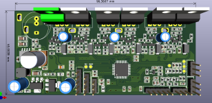
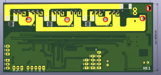
Hello everyone,

Just a quick update:

I’ve completed the initial design for the motor controller. If you notice any areas that could be improved, please feel free to share your suggestions—I’d really appreciate your feedback!

I’m now in the process of selecting a low-cost MOSFET suitable for a 42V, 350W e-bike motor. If anyone has recommendations for reliable and budget-friendly options, I’d love to hear them!

Thanks again for all the support!
Best regards,

BldcLover
1748718255960.png
1748718279103.png
1748718155160.png
1748718135684.png

1748718180781.png
 
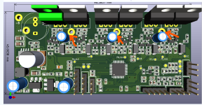
You might want more spacing between those capacitors and the wires soldering area, there is a change the capacitor body might touch that area. When you will solder the wire you might damage the capacitor plastic wrap and expose the bare metal.

If you shrink wrap the capacitors base or protect is somehow else this might be OK.

1748729349910.png
 
You might want more spacing between those capacitors and the wire soldering area — there’s a chance the capacitor body could touch that area. When soldering the wire, you might accidentally damage the capacitor's plastic wrap and expose bare metal.
If you shrink-wrap the capacitor base or provide some other form of protection, this might be acceptable.
Thank you for the helpful observation. Actually, I will bent the capacitor slightly toward the diode to make the wire soldering process easier and to maintain clearance. However, I’ll ensure there’s adequate spacing and consider additional insulation — such as heat shrink — around the base of the capacitor to avoid any risk of damage or shorting. Appreciate the reminder!
 
INA181 with groud plane ,
1748974623365.png
1748974651279.png
1748974670468.png

3.3vdc supply top and bottom view,
1748974682425.png
3.3VDC Supply to INA181 , top layer
1748974692187.png
3.3VDC Supply to INA181 , bottom layer
1748974704920.png
1748974731673.png
+12vdc top view
1748974754572.png

+12VDC to bottom view,
1748974764440.png

Layer 2 as ground plane:
1748974774171.png


Now I am confused — should I use large polygons for 3.3 VDC and +12 VDC in layer 3 as power planes, and keep the +Battery trace routed externally, or should I replicate the same strategy on the power layer?


Here is the my github repo:
 
Depends of what is easier to trace and how many consumers of each voltage. I guess 12V goes only to one spot where it is reduced to 3.3v and 3.3V goes to many places? If so then it is easier to trace 12V with one thick trace to the place where it is dropped down to 3.3V and from 3.3v source make a power plane where the 3.3V consumers will take the power through vias from the 3.3V plane.

There is no reason to do power plane for the voltage if there are only few consumers of the voltage and they are close to the source of the voltage and you can simply make a short trace to them. Power plain might be necessary only if it reduces the tracing work and amount of the traces spaghetti or if there is a risk you can shorten power to something during handling the powered PCB then you hide the power inside the PCB in power plane.
 
Last edited:
Back
Top