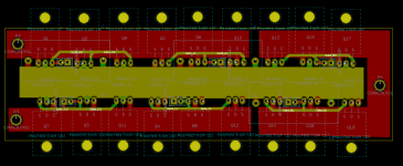
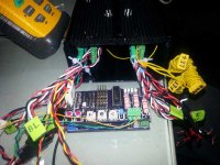
My new 18 FET TO-247 layout riding video page 10

to know how much ringing is too much, its a balancing act. you don't have the lab equipment to make that decision quantitatively. it very similar to switching fast which is good cause lower losses but higher noise which is bad. here you might have the equipment necessary to measure that relationship quantatively but you can just use experience instead. generally at your power range you should be switching 200ns to 300ns range. but its not an exact science.

if you were switching sub 200ns and 600A as your continuous operation, that's something else. that i would say is beyond your system's capability. doesn't mean you can't do it, your gate driver is good enough that it might be funcitonal.. but its not really designed for that level of noise. you'd have to change to more advanced interface to protect the lewbowski brain.

Trying to get 15-25 parallel devices to play nice together should be a challenge
that's on the To-Do list. let me know when you're ready to learn VHDL programming and i will show you a way to make this work. well, maybe not that many, but between 8-12 per switch should be possible.
 
zombiess said:
Everything is hooked up, now I'm trying to get the controller to spin the motor.
As an engineer (not EE) who's dabbled in electronics just a little, I am quite interested in this thread. It's not very often you read an entire thread and the last post is "oh and I'm about to test it"! Very exciting stuff. A few pages back I saw you were looking for a riding buddy.. My bike won't be nearly as fast as yours (yet) but I'm located pretty close in Bakersfield and am always down for a trip to Ventura. Here's to hoping your test was successful!
 
AustinP said:
zombiess said:
Everything is hooked up, now I'm trying to get the controller to spin the motor.
As an engineer (not EE) who's dabbled in electronics just a little, I am quite interested in this thread. It's not very often you read an entire thread and the last post is "oh and I'm about to test it"! Very exciting stuff. A few pages back I saw you were looking for a riding buddy.. My bike won't be nearly as fast as yours (yet) but I'm located pretty close in Bakersfield and am always down for a trip to Ventura. Here's to hoping your test was successful!


If you meet with Zombiess, you won't need to have a slow bicycle anymore. :)
 
Controller is working now, I spun a Cromotor after troubleshooting a bad solder joint and a minor wiring mistakes I made.

Now I need to put it in the case and tune it so I can try riding it.
 
zombiess said:
Controller is working now, I spun a Cromotor after troubleshooting a bad solder joint and a minor wiring mistakes I made.

Now I need to put it in the case and tune it so I can try riding it.

So exciting!! This controller should make a stupid fast ebike!
 
liveforphysics said:
zombiess said:
Controller is working now, I spun a Cromotor after troubleshooting a bad solder joint and a minor wiring mistakes I made.

Now I need to put it in the case and tune it so I can try riding it.

So exciting!! This controller should make a stupid fast ebike!

Especially for those of us who need two. :twisted:
 
Tested the different current sensors today. As expected the 100A (300A) sensors are working well. Switched over to my 200A (600A) sensor and they also work very well. For giggles I tried out the 600A (1800A) sensor and they did not work, but at 1.042mV/A it's not any surprise. At low current the signal is going to be lost in the noise.

Now I need to put this into a case. Sadly I ran into an size issue that is going to prevent me from putting the brain in the same case this time around. I had to modify my gate driver boards due to a minor design error on my part that cascaded into other changes.

The next design will be much better.

I hope I'll be able to start test riding this tomorrow, but I have to sort out my error handling PIC to make sure everything is safe and the PWM latches off if a fault is detected.
 
I didn't manage to get the controller into it's case yet :(

Nothing is wrong, I just wanted to experiment with it on the bench some more. I have the controller dialed in as good as I'm going to get it on the bench. Need to load it down now and ride it.

It's going to have to wait until next month now.
 
Booooo….

:p
 
HighHopes said:
Booooo….

:p

Says the guy who works so many hours he has little time for his own projects :mrgreen:

I'll be working on some simulations for the next few weeks. Tomorrow I have an 17hr flight + airport time I need to kill. Maybe I can simulink myself to sleep.
 
Hi. Just wanted to let you know that you have another interested follower here.

After my building my first electric bike last summer, things started to escalate pretty quickly and now I have started planning on building a real electric motorcycle. In order to get the best performance, I would probably be using a brushless motor, which requires en expensive controller. Since i've made some controllers for small brushed motors, I thought why not design and build also my own brushless controller. After reading this thread and a couple of others for the past four hours, I decided to forget that idea. Well, at least the designing part. I really did not realize how much work it would take to choose and fine tune the components when the power levels are above 10 kW. Its great to see professionals like HH helping open source projects like this.

Anyway, points for you for the thorough fine tuning work. I am waiting to see how the controller works in a bike. After this much bench testing, I'm sure there will be no problems. Personally, I would have built the controller, put it in a bike and checked the connections after the smoke had cleared.

I think I could use this power stage to power a ~30 kW peak brushless motor such as Motenergy ME0913 at approximately 100 V. I guess four or five IRFP4568 FETs in parallel could be adequate. The power stage layout looks nice, I like how easy it is to mount the FETs to a large heat sink. I would probably mount the controller inside an aluminum battery box without a separate enclosure.

There are a couple of things I am wondering:
Does also the DC link cap have to be polypropylene? Is it not enough to have a few uF of snubber cap and a electrolytic cap as DC link? An electrolytic cap would be much more compact an would allow reducing the size of the PCB.

Is it really useful to make a 4-layer power stage when there are only the secondary bus conductors in those layers? Do they even conduct basically any current since their resistance is much higher than that of the top layer conductor and bus bars? A two layer board would be cheaper to produce (from Seedstudio, Itead etc.).

Have you calculated how significant the switching losses are? Is it necessary or beneficial to have the booster even when more FETs in parallel cause a slightly slower switching?
 
all good questions and zombiess will answer them i'm sure when he's free.

I really did not realize how much work it would take to choose and fine tune the components when the power levels are above 10 kW.
don't feel alone on that one.. NOBODY realized how much work and knowledge it takes to make a real product 10kW or higher actually "work" (work = functional + reliable). its why you have never seen (until now) an open source project of any quality on the subject. look around the net.. hard to find any and of the few you find, i think none are at this level, not by half.

but i think once zombiess is done his playing around, we'll go back and properly document how this is all done. with all the knowledge built into chronlogically "easy" to follow design methodology for the basic high performance motor drive. once you have all the info spelled out like that, i think someone with your desire and interest would have the confidence and enough knowledge to make a real go of building your own.

here's the KEY. the first time you build one, follow ** EXACTLY ** the advice given from a professional even if it sounds wasteful. you must learn first how to do the thing properly before you try to optimize it on your own for your own reasons. yes its slightly more expensive and/or bigger to follow the instructions.. but remember, there's never been open source like this before for a reason. you have to build the correct thing first so you can learn what has never been shared before so you can appreciate why things are the way they are. this work is harder than zombiess makes it seem. there is A LOT going on behind the scenes that you do not see. lines and lines of math, 3D electromagnetic field containment/mitigation, failure mode analysis, tradeoff decisions of design etc etc. after you see that, THEN you are free to make the changes as you need for your purposes. at leaset then when you make the changes you will understand how to make those changes such that you still will end up with a working product.
 
Thank you HighHopes. The revolution in DIY EV powertrain density is now happening now largely because of your contributions, and the hard work of only a handful of passionately dedicated ES'ers who created a priceless open and free education path for those in the E-revolution world wide.
 
T.J.L. said:
There are a couple of things I am wondering:
Does also the DC link cap have to be polypropylene? Is it not enough to have a few uF of snubber cap and a electrolytic cap as DC link? An electrolytic cap would be much more compact an would allow reducing the size of the PCB.

Is it really useful to make a 4-layer power stage when there are only the secondary bus conductors in those layers? Do they even conduct basically any current since their resistance is much higher than that of the top and layer conductor and bus bars? A two layer board would be cheaper to produce (from Seedstudio, Itead etc.).

Have you calculated how significant the switching losses are? Is it necessary or beneficial to have the booster even when more FETs in parallel cause a slightly slower switching?

The DC Link capacitor type was chosen due to the price being almost even. Eletrolytics can be used, but often times several thousand microfarads are required which increased the volume the capacitors take up. Since the RMS ripple current is the main design criteria to meet, using parallel polypropylene capacitors with higher current ratings makes sense. The design of the controller is to last +10yrs minimum. Controllers can place a large demand on capacitors from many heat cycles up to 80C inside the case. Polypropylene capacitors also have self-healing properties if damaged with the only downside being reduced capacity.
I just checked my ripple current calculations and this controller will place a 16.8A RMS ripple current demand on my capacitors. It would take at least six 330uF Nichicon CS Series 105c 10,000hr rated 3.1A ripple capacitor to meet the current demand. The price is lower than the Polypropylene capacitors I chose, but I want to use the best components since there is not much overall cost difference for the benefits gained from PP. The load was spec'd for 50uH, 21kHz PWM, 50% Duty.

The 4 layer board was chosen in an attempt to reduce EMF/RFI from the power pass. I do not know if it works as intended yet as I don't have a control to compare it to. I was unable to create a fully laminated bus bar layout which means I have more EMF that is not canceled out to worry about. This EMF interacts with the stray inductance within the rest of the layout. If you look at the last pictures I posted there are two that relate to this issue. The one picture shows an unpowered adjacent gate driver with 0.6v on the gate-source connection w.r.t. it's ground reference. The IRFP4568 has a gate threshold of around 3V so I'm still safe, especially since the measurements were taken at 500A and this controller will only see somewhere around 300A phase for a short period. Still, having voltage being picked up by the gate on adjacent MOSFETs is not a good thing. That is why the gate driver has a Miller clamp as can be seen in the 2nd picture where the gate driver was powered on to activate the Miller clamp. That 0.6V drops to a 0.4V spike that is then held to ~100mv. I'm not sure how much of the spikes seen are real, some of it is common mode noise from the scope.

The RFI comes from switching very quickly, I'm currently < 200nS which is quite fast. This reduces switching losses, but increased the noise due to the rapid rising/falling edges of the D-S voltage. The thought was to stop some of it with the inner copper layers going to the respective grounds. My next layout will feature a fully laminated bus bar system and only us 2 layers (that's the plan at least). I'll make the same measurements when I build it.
The boost stage was done because I wanted to test it in a real application. I've verified it can deliver 15A in a previous test. While I don't need 15A, the TD350 is only able to source 1.5A for turn on and sink 2.3A for turn off. With my very fast switching times I have 15V/6.5ohm = 2.3A on and have to sink 6A at turn off. The 0.5 ohms on each resistor is due to using 6.5 ohms at each gate to dampen any ringing.
I have a spread sheet to help me do the switching losses that I created, but I have not estimated the losses yet. I should do that as I am curious. I am current unable to estimate the reverse recovery losses from the body diodes during hard switching, but once I do some final double pulse testing I’ll at least have a scope shot to go off of. In the mean time I'll calculate the switching/body diode/conduction losses with a Tj=150c aiming for a worst case scenario.
Thanks for following along. If you do decide to try your hand at this, take good notes and listen to pros like HighHopes. It's best to do it their way even if you don't understand why. Things become much clearer as you start learning the physics at play. Layout is certainly an art form because you must think in EM fields.
 
Thank you HighHopes. The revolution in DIY EV
and we're just getting started! if you have the interest for it, we'll tackle all the issues together until a full, but basic, system is described from beginning to end.

perhaps the next major build thread will be like this "i'm going to use zombiess gate driver and spend my time designing a better interface". and we'll build on the good we have already accomplished here to take the system design that next step farther. who wants to volunteer to will kick this off?
 
zombiess said:
The 4 layer board was chosen in an attempt to reduce EMF/RFI from the power pass. I do not know if it works as intended yet as I don't have a control to compare it to. I was unable to create a fully laminated bus bar layout which means I have more EMF that is not canceled out to worry about.

I've been thinking about the layout for the power stage for the past couple of days. I am not familiar with laminated power buses but to my understanding it means placing conductors with opposite current directions close to each other so their magnetic fields counteract each other. If that's the case, apparently it would be best to place the bus bars for the battery connections in the same position but on different sides of the pcb. Best would be to cover the bus bars with ground planes on the outer sides but with a one pcb design it is obviously not possible. If the power bus bars are in the middle of the high and low side FETs, it will be difficult to connect both FETs to the phase out connection. Therefore I thought why not place the FETs for one phase in one row.

I created a quick layout in KiCAD. It's made with TO-220 footprints since I did not have a suitable TO-247 footprint and it does not contain all the resistors, capacitors etc. Actually the FET legs might also be wrong order but it really does not matter now. What do you think about this kind of layout? The power buses run in the middle with phase A FETs above them, phase B FETs below the buses and phase C FETs on the right. The phase wires could be soldered on the front layer zones above the FETs. The three large caps are placed right next to (partly on top of) the power buses.
power_stage.PNG
This kind on layout would allow for the fully laminated power bus, however the phase currents travel a bit longer route on the pcb. Especially when I would build this with five FETs in parallel instead of three like in this example. This would be quite a different approach to the one proposed by Lebowski. What are your opinions?

What about your next fully laminated layout zombiess? Mind sharing it so we can all give it some thought?
 

Attachments

  • Power stage.zip
    38.6 KB · Views: 35
T.J.L. said:
I created a quick layout in KiCAD. It's made with TO-220 footprints since I did not have a suitable TO-247 footprint and it does not contain all the resistors, capacitors etc. Actually the FET legs might also be wrong order but it really does not matter now. What do you think about this kind of layout? The power buses run in the middle with phase A FETs above them, phase B FETs below the buses and phase C FETs on the right. The phase wires could be soldered on the front layer zones above the FETs. The three large caps are placed right next to (partly on top of) the power buses.
View attachment 1
This kind on layout would allow for the fully laminated power bus, however the phase currents travel a bit longer route on the pcb. Especially when I would build this with five FETs in parallel instead of three like in this example. This would be quite a different approach to the one proposed by Lebowski. What are your opinions?

What about your next fully laminated layout zombiess? Mind sharing it so we can all give it some thought?

You have the understanding of a laminated bus, that's a rule and a very big one. This is a very difficult game to play without knowing the rules and scouring the internet will only provide bits and pieces with large chunks missing. This site has more info than any other location I've seen, but it's very hard to find all the good stuff since without having a feel for the rules it's hard to discern good info from bad :( A classic chicken/egg scenario. My build threads and Arlo1's build thread has good info, I'd stick to HighHopes comments for the most part.

I've been compiling notes (well over hundreds of pages to sort through) from discussions I've had with the knowledgeable designers on this site. The largest contributor being HighHopes who has been doing this for > 10yrs in an industry that has VERY high specs to meet. I'm also adding my own notes as my understanding grows, I'm passionate about this field and have started digging into the details. It sounds like you have a strong interest as well based on your questions.

My first build took me an entire year of him tutoring me several times per week and I didn't start off as the most patient but quickly changed my tune once I saw how valuable it was. I'm trying to pay it forward myself now and feel pretty confident about the basics. It works quite well. My 2nd build (this thread) is a vast improvement and my upcoming 3rd/4th builds will be yet another leap.

The new bus bar layout will feature water jet cut copper 1/8" thick, 0.75"-1.00" wide DC bus bars separated by kapton tape. Only a small fraction of the bus will not be laminated. They will be placed on the same side of the PCB allowing phase out bus bars on the other side to resist PCB warping and facilitate high current output. I'm sorry I don't have a diagram yet as I'm no 3D modeler.

Since you asked for a critique on your layout, here it goes.

You are at the same design issue I was in about 1yr ago, parallel devices really limit layout choices. It took me a long time and many iterations to come up with what you see in this thread and it's only been in the last 4 months that I figured out how to improve on it and meet the fully laminated layout design rule. For low power <1kW to probably 5kW you can get away with bad rules. Heck I've done short bursts of 25kW @125V on a Xie Chang 36 MOSFET controller which has an atrocious layout and the worst gate driver performance I've seen (now that I understand what I'm looking at), but I wanted something better.

Your DC bus layout will work fine, I did the same style on my first controller, one on top of the PCB, one on the bottom. The issue is the phase output and the gate trace routing. Each gate trace needs to be over it's respective ground reference to prevent the stray inductance in the gate traces from picking up the EMF and converting it to voltage. That voltage can then raise to the gate threshold causing an adjacent non active bank to turn on causing a shoot through event. The gate driver design / layout is critical to the success of any controller. Your gate traces violate the rule of never routing them into the power pass section. The power pass is your DC Link and phase output (all the power passes through these areas). It looks like you planned to use twisted pair to connect to the gate traces, that's allowable since the gate signal has it's respective ground reference.

I see what looks like some large caps, I'm guessing they are DC Link? What about the snubber caps? It might be better to place DC link caps right at the entry of the battery pack feeds. I'm not sure and I think I remember HH and myself discussing this and we ended up undecided on if it was OK, but he has never done it before. He has also had limited experience with paralleling which has lead to some interesting discussions on some findings I've made and he added additional info I didn't know that was happening (all positive effects). IMO it's OK to distribute down the bus, I know it works as Sevcon does it with lots of little electrolytic caps and no DC link caps (not a fan of this), but it's certainly functional and appears to work (works = functional + reliable). One issue that could happen with running them down the bus is any stray inductance could setup ringing between the caps on the bus. I personally have not seen this during testing, but my designs are fairly low inductance. I'd suggest copying my layout as it allows for low profile and a large heat spreader or heat sink to be utilized and I spent a lot of time figuring out what looks like an obvious layout (rules and details). I'm very fond of mounting the MOSFETs flat. It is important to keep all parallel MOSFETs on the same thermal mass. Looks like you'll be mounting them all on the same sink which is good.

You also might want to tie your gate pin to your source pin with a resistor if you haven't done so already. Somewhere around 4.75k is usually good. The reason to do this is to control the state of the gate during power up/power loss. HH gave me the math to prove this, but I think it or myself has an error. The goal is to make sure you can control / know what state your gate is in at all times aka what happens if your gate driver loses power while running, will something pop?

Symmetry is also important, keep that in mind when designing. Everything about power electronics is detail oriented, so many rules. HighHopes an myself have plans to write a how to, but we both need some more free time as it's not going to be a short story. I'm already collecting information by keeping good notes and snagging the math from white papers, thesis papers, app notes, etc to justify design choices.
 
Got some more of the controller work done.

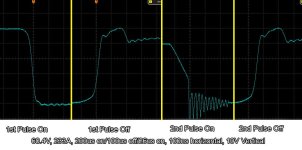
Did some double pulse testing, here are the results.
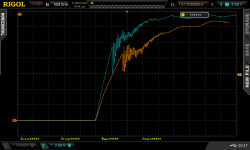
I have turn on ringing on the 2nd pulse which from what I can tell is normal. What I find interesting is the ring frequency changes compared to the 1st turn on.

Tests done with 6.2 ohm on resistor, 2.0 off resistor
Double Pulse 60.4V @ 233A 200us on, 100us off, 26us on
Initial turn on ring 5.7 Mhz, Turn off 5.9 Mhz
Turn on ring at 23.8 MHz turn off ring is at 5.9 MHz

double-pulse.jpg

This shows a comparison of a 6.2 ohm (blue) gate resistor vs a 10 ohm (orange) gate resistor. Since they were essentially they same I went with the 6.2 for the increase in switch speed (not shone in this shot). I lost the one I did with the differential which shows a bit less ring. My setup doesn't let me use a short ground probe, had to use the long one. At least I have reference shots to compare to on the next build.

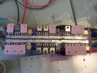
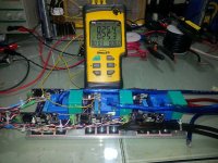
Decided to do some more data logging and get a better idea of the thermal management of the MOSFETs themselves. I placed a probe on the MOSFET leg, another on the body and another in the ambient case air.

01-Temp-Probe-Leg.jpg

02-Temp-Probe-Leg.jpg

That metal tab is compressing the thermocouple against the MOSFET body
03-Temp-Probe-Case.jpg

View attachment 4

My thermometer will show the delta in MOSFET leg/body
05-Temp-Probe-Delta.jpg

All the wiring made a bit more tidy. Yes that's hot glue holding stuff in place for now, needed to manage the wires somehow so I could slide it into the case. It might melt if I let the internal temp get over 80C which I do not plan to do. Labeled all the wires coming out so I hopefully don't mix them up (again). All low voltage wiring is twisted to help lower the inductance.
06-Wired-Up.jpg

Everything slid into the case. Without fail, not everything will fit. I figured that going into this though since I knew I would have to make changes on the fly. The brain board will be placed into a separate case.
09-In-the-Case.jpg
 

Attachments

  • 14 10r_vs_6r2_g_s_on_2nd_pulse.png
    14 10r_vs_6r2_g_s_on_2nd_pulse.png
    9.5 KB · Views: 2,420
have you ever considered putting an AC filter on the output to filter out the switching noise? i'm not saying you need something like that, but, as an experiment, it would be interesting to see what benefits such a thing can bring. mostly, i'm curious if there would be a noticeable torque increase? there are other benefits too but not so easily observable. of course the big downside is increased cost & volume so the benefits have to be very high to make up for it!
 
HighHopes said:
have you ever considered putting an AC filter on the output to filter out the switching noise? i'm not saying you need something like that, but, as an experiment, it would be interesting to see what benefits such a thing can bring. mostly, i'm curious if there would be a noticeable torque increase? there are other benefits too but not so easily observable. of course the big downside is increased cost & volume so the benefits have to be very high to make up for it!
Like inductors on the phase leads??
 
that's right. if you put JUST an inductor, that would be a first order filter (the motor itself is also a first order filter). if you put some capacitors after which is then a LC filter, that would a 2nd order filter and more in line with what i was thinking. the MAIN reason peeps put one of these filters on is so you don't beat up your motor with vvery high dV/dt switching and a close 2nd reason is to reduce EMI (which is not that important to a DIY'er who doesn't have specs to meet).

you can also put a common-mode LC filter too (this would be a second LC combination) which is really more for ground circulating current reason, i.e. safety. i think this is not really needed at all in an EV cause, correct me if i'm wrong, the battery's negative terminal is not chassis grounded to the frame of the car/bike.
 
HighHopes said:
the MAIN reason peeps put one of these filters on is so you don't beat up your motor with vvery high dV/dt switching and a close 2nd reason is to reduce EMI (which is not that important to a DIY'er who doesn't have specs to meet).

How much does the noise dV/dt beat things up? It would do it through capacitive coupling, correct? Is the ringing at the resonant frequency of the motor/controller circuit or are you talking about? Would this be the resonant freq of the motor / wire inductance and any stray capacitance that exists in the circuit?

Have you ever seen capacitive coupling damage yourself or just stories/papers on it? I haven't found much on the subject, but I understand the cause.

EMi isn't nice, but I am concerned about addressing it, but currently lack the test equipment to categorize it. What about noise that is conducted back into the traction pack? I haven't thought much about what this could do to a battery. I know it's a concern on grid tie systems which need to meet FCC Part 15 B and UL1741. I'll ask our local battery expert LiveForPhysics.
 
Back
Top