My new 18 FET TO-247 layout riding video page 10

when you post videos of ripp'n around town in your new controller it will make a 10 fold increase in number of downloads. until then your controller has some quality to it and the discussion, most of it in PM form but some posted here, is a rare find on the net. those that can recognize such things are probably following along. looks like there is a fair number of them. wish they would join the conversation too :)

we're putting this all out there in open source for all to learn. the discussion so far is a bit jumpy, but eventually it will get re-typed in a much more clear step-by-step. we're working on this in the background (amongst many other things). then everyone will have the complete story of a quality inverter built. theory, analysis, architecture, detail design (including PCB design), development test. we'll leave out qualification test and other subjects such as designing for manufacture, or designing for cost for now. i hope we can get a chance to include discussion on software design, also open source, but that will have to wait for a bit.. still more work needed there before comfortable discussing in open thread. a lofty goal, but i really hope it happens :)

ps. my EV motor drive schematic, still in development, has had over 7000 views!
 
When you have this refined and running as an essentially unblowable high performance motor controller, folks are going to be buying you out of PCB's to make them.

This will be the case with Arlos controller as well. The world has been missing these hotrod BLDC controller options.
 
zombiess said:
I believe more than just the few of us posting are reading.

Hope everyone reading is having fun learning as I progress.
I believe less than just the few of us reading know what you are writing about just in hope to see finally reliable controller. :D Thank you for seeding hope.
 
I found my noise source by process of elimination. There is a lot of EM field coupling between my differential probe amp (it's external) and the actual controller (not the coil). This probe setup is really designed for lower voltage digital work, not power electronics, but I got what I got.

I minimized the noise by experimentation. I distanced the controller and the amp as far as I could and then rotated it until I found the position with the least coupling. I then started bringing the probe near the controller, no change in the signal level so the probe doesn't appear to be succeptable. I was then able to start making measurements and start seeing what's going on.

Of interest to me is the bump that happens on the gate-source right after the drain to source turns off. It's very current dependent. I've seen this before on my previous setup. It's not high enough to turn on the opposite side and cause shoot through. I'm testing this setup at much higher pulse currents than I plan to run it at. The signals I'm seeing are much cleaner than those I saw on my previous design which was tested at 1/4th the current I'm using now. I'm pretty confident this setup is going to work well for the power level. The improvement over my first design is quite significant. The 3rd design is going to be even better!

I'm going to bump my voltage up to 96V and do some more pulse testing with a 25uH coil to simulate a hard to run motor. I'm feeling good about using this controller based on this design on a motor like the Colossus.

I'd really like to do some testing under real life scenarios of running a motor to see how motor dynamics effect what's going on. Starting a motor from a dead stop with a WOT command vs going WOT once it's rotating is a different scenario. I hope to get the controller back in it's box by next weekend and try running it, just need to do a few more pulse tests.
 
Excellent work my friend! Excited to see things moving forward, and great job learning how to get these tricky readings.
 
Jeremy I think I saw the bump before in my working 18 fet controller it was just as the current is trying to flow through the fet diodes to the caps and adding good caps in the right place helped make it better. Get us some screen shots. :)
 
So I just wanted to update that my previous scope shots are pretty useless except for showing how difficult it is to get a good view of what is going on in a noisy environment. My probes are picking up way to much noise for me to figure out what the real story is. I'm going to have to do some research and see if there is a better way to measure. The EMF field the controller and coil are producing is just too much to handle. I've been doing some reading on magnetism and I think what I'm seeing is H field coupling.

I did some more pulse testing with a passive probe floating, with a normal ground lead attached to the tip and with aluminum foil shorting the tip to the ground. All of them pickup the field and create noise hiding what is really happening. I can make the noise switch phase by rotating the probe in certain configs. I'm believe the probes must have too much stray inductance.

Anyone have a good idea on how to get cleaner measurements? I'd really like to see if there is a chance of false turn on in the opposite gate diver.

One thought I had is to position the probe with the tip grounded as close as possible and held in the same position I'll be measuring to the test point I want to measure and then take a reference shot and save it on the scope. Since the probe is grounded, anything that shows up is going to be noise from the test setup. Then I can make my measurement and subtract the reference waveform from the measured wave form, this should be really close to the actual signal.

Another idea is to try using the two probes and make a poor mans differential measurement and see if that works any better.

Making measurements like this is a challenge in itself.
 
Are you still testing with an air core inductor? Maybe try putting it in a metal box? Or try a Ferrite core as an air core will emit a lot more noise.
 
Arlo1 said:
Are you still testing with an air core inductor? Maybe try putting it in a metal box? Or try a Ferrite core as an air core will emit a lot more noise.

I tried moving the coil far away 3m which helped a bit, but having a probe right over the bus bars and MOSFETs is still an issue.
 
I would be tempted to make a small differential amplifier based on a differential amplifier IC and position it very close to the signals with short twisted pair to bring the signal. Shield it, but get it very close to the signals, avoid all the long low level leads. After the signal is buffered it can drive a coax to the scope through a short length of good coax. Soft reference it to circuit ground using a resistor to avoid pickup from the noise on the ground, but to keep the common mode voltage within range of the diff amp.

Twist the wires feeding the coil to reduce radiation.

The length of the leads picks up H field signals, making them very short and twisted helps a lot. Use a small battery right at the diff amp to power it. The goal is to reduce/eliminate all the signal pickup antennas.
 
@ zombiess
Let me know when you run your next batch, I will pay for an extra four (plus 4 small controller).
Cheers
 
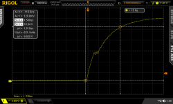
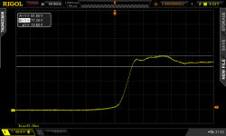
I've been analyzing some stuff on the bench for the past week. I've known for a while that my 10 ohm ON gate resistor is too high for 3 parallel MOSFETs as my G-S on time from 0-10v was slow, 1.6 us slow.

The following shots were all taken with 300A pulses at 64v bus.
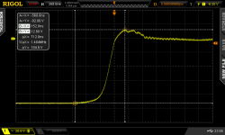
Lazy on time with 10 ohm gate resistor
01 10r_g_s_on_1.png

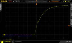
Dropped down to 6.3 ohms
02 6r3_g_s_on_2.png

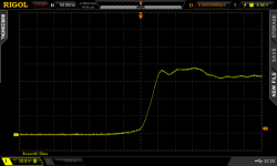
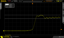
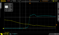
Then went down to 4.7 ohms and got a tiny bit of ringing after the Miller Plateau (any thoughts on this, is it too much?) I think the ringing freq is tied to the G-S cap.
603 4r7_g_s_on_3.png

I started out with a turn off resistor of 4.7 ohms. I had tried going lower previously, but was not happy with the overshoot at turn off. I decided to do some more investigating into the turn off overshoot and found out that it's caused by switching speed, the turn on of the freewheeling diode + it's lead inductance and the lead inductance of the MOSFET + PCB traces. The overshoot happens after the D-S is complete and the freewheeling diode takes over the current. I've seen as high as 30V overshoot with a 24V bus. As the bus voltage is increased the overshoot starts to dispensary. It's most pronounced at low bus voltage. I also noticed that the width of the overshoot is determined by the amount of current, more current = wider overshoot.

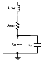
The overshoot happens after the D-S goes to an open circuit. What is left is the freewheeling diode + all the stray inductance and the D-S cap (Cds) of the MOSFET which is now off. This is a diagram I found of what it looks like electrically... a tank circuit. This explains the ringing that is often seen if it is left unchecked.

effective circuit.png

This was found in this PDF as well as the above explanation. The PDF describes a method for reducing turn off overshoot by using an op amp, but I've been able to get good results by adding a single gate-source capacitor which is much simpler than the proposed method. I don't fully understand how it's working yet, but it does and I've got gate driver current to spare.
View attachment Gate charge control for MOSFET turn off.pdf

Here is what my D-S turn off looked like with the 4.7 ohm resistor.
04 4r7_d_s_off_2.png

I ended up at 2.0 ohms
05 2r0_d_s_off_2.png

The first step is the 2 level turn off, 2nd is the miller plateau and finally the miller clamp around the 1V mark
06 2r0_g_s_off.png

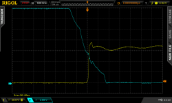
This is the G-S vs the D-S at turn off
07 2r0_g_s_vs_d_s_off.png

My overshoot is not too bad as can be seen. It's limited to a max of ~18v with a 64v bus and a 300A discharge. I was surprised by how much the G-S cap effected this and overall ringing both at turn on and turn off. I was originally at 33nF in my previous test but tonight I upped it to 68nF to see what effect it had. I had tried to drop the 4.7 ohm lower but the overshoot and ringing got to be more pronounced.

This is the 33nF G-S cap with a 4.7ohm turn off resistor. Compare these shots with the above using the 68nF G-S and a 2.0 ohm turn off resistor. The 33nF/4.7 ohm has more overshoot and ringing than the 68nF/2.0 ohm combo. The 68nF/2 ohm setup turns off about 25nS slower D-S, but has much less ringing after the turn off spike. The G-S switch off event is cleaner as well.
08 33nf_d_s_4r7_1.png

I'm quite curious to find out how the G-S capacitor is functioning to stop the overshoot/ringing. I need to simulate it or scope around some more to see if I can make more sense of it. I'll remove the G-S capacitor completely and go back to 10/4.7 resistors for on/off and get some scope shots to see what things look like (it won't be pretty, I've done it before).

33nF G-S cap with 4.7 ohm off resistor
09 33nf_d_s_4r7_2.png

This gate driver/power stage setup has much better looking wave forms at 300A than my first 4 parallel power stage did at 325A with 95V bus.
Here is a picture of 4 parallel IRFB4115s switching 325A at 95V bus.
10 old d_s_off_95v_325a.png

What do you all think of the switch times and shape? Thoughts on running a big G-S cap like I am experimenting with?
 
your comments are all about right and your understanding is good. these waveforms are about as good as you can get with your setup wich is more than acceptable.

the switching time is not your G/S waveform, it is D/S that matters. i would say its better to have slower G/S with minimal rining then fast G/S with ringing. this is because the D/S switching time is probably the same in both scenarios which is the part that matters but you don't want the ringing to carrying through. mosfet losses are based on D/S switch time and production of EMI is based on D/S switch time.

G/S switch time is only indirectly affecting d/S switch time. the mosfet will have a switch time of its own once G/S voltage reaches threshold value.

also, your switching frequency, still around 20kHz? so you can get by with slower G/S and no ringing.. you don't need blazing gate driver. It's possible to swing the kind of power you want at 100kHz switching frequency but not with your current design's technology and implementation (but you already know this).

anyway, what you have now is more than sufficient for your needs.. so Bravo! another high quality gate driver reaches the open source world! and believe me, i know a bad one from a good one.. this is a good one. probably only one of maybe 5 that exist in the world that is open source :)

so what are you going to do next?
 
HighHopes,

You wouldn't be too concerned with a 1.6uS G-S on time going 0-10V? Seems a bit sluggish, but I've seen controllers run way slower than this at 16kHz. I know the key switch time is the D-S, but what happens if the G-S time is really long, say 5uS to go 0-10V, isn't there some point where this can become an issue?

Looking at the D-S voltage I'm turning completely off-on in ~125ns and on-off in ~100ns, seems pretty fast.
This controller will most likely have a max Fsw of ~21khz, but I plan to run the Fsw as slow as possible to minimize switching losses. No need for 21kHz if the motor runs fine at 12kHz.
 
zombiess said:
HighHopes,

You wouldn't be too concerned with a 1.6uS G-S on time going 0-10V? Seems a bit sluggish, but I've seen controllers run way slower than this at 16kHz. I know the key switch time is the D-S, but what happens if the G-S time is really long, say 5uS to go 0-10V, isn't there some point where this can become an issue?

Looking at the D-S voltage I'm turning completely off-on in ~125ns and on-off in ~100ns, seems pretty fast. Is this under load? because that will effect things
This controller will most likely have a max Fsw of ~21khz, but I plan to run the Fsw as slow as possible to minimize switching losses. No need for 21kHz if the motor runs fine at 12kHz.

The time a gate takes to go to X amount of voltage doesn't really matter. Its the time the drain to source takes to transition. The way I see it is every mosfet/IGBT will have a different start and end point for the D-S transition in relation to the gate voltage so if you know this number exactly (which changes with heat) you can try to measure the time in the window (miller plateau) but its very hard to be accurate from so the best way to measure the time is watch the transition on the D-S.
 
The above scope shots were taken at 270-300A load at room temperature ~25C single/double pulse. I did heat stuff up a bit with my SMD rework station, probably 60C, didn't see much change.
 
zombiess said:
I did heat stuff up a bit with my SMD rework station, probably 60C, didn't see much change.
What I mean by temp will change it is it will change the start and end point of the transition for the D-S in relation to the G-S as well as possibly changing the curve through the transition.

D-S is what you care about...

IF you have 2v on the gate and the D-S is still open and has not started its conduction yet then the 2v means nothing.
Just like -5v means nothing when you are pulling it to -8 or -9
The voltage on the gate before and the voltage on the gate after the transition doesn't mean anything. What you care about is the transition though the trans-conductance zone as this is the time you produce the most heat and you need to keep an eye on it for ringing.
 
HighHopes said:
this is because the D/S switching time is probably the same in both scenarios which is the part that matters but you don't want the ringing to carrying through. mosfet losses are based on D/S switch time and production of EMI is based on D/S switch time.

G/S switch time is only indirectly affecting d/S switch time. the mosfet will have a switch time of its own once G/S voltage reaches threshold value.

I read that reducing the turn off overshoot (which I did with the G-S cap, but I don't yet understand the physics) improves switching losses (bonus) and also reduces EMI (double bonus!). I can increase my G-S switch time and make those traces look buttery smooth, I think the sweet spot is 7.5ohms
 
you have some room on G/S switch time. think of it as a delay. and then you will see the issue.. deadtime. your deadtime has to account for this delay. but your gate driver is really well designed so you do not have the problems that cheap ones have, you have the problem that good ones have which is this "there are no bugs i have to work out, there are no crappy anythings, i just have to tune it" which is what you are doing by fine choosing values of resistor & caps. its exactly how it is supposed to be.

did you go through all your fault modes and see how long it takes to detect said fault and how your brain responds? did you suddenly drop your gate driver power supply and see what happens? what aabout gate driver power supply under voltage? does your brain restart automatically or does it have a 250ms rest first (that's controllable in software) or does it latch off permanently under reset. what state is your gate driver in at power up? power down? what if your gate driver gets power before your brain does?

there's still more you can do but it will go beyond the "basics" of a good working gate driver.
 
HighHopes said:
1. did you go through all your fault modes and see how long it takes to detect said fault and how your brain responds?
2. did you suddenly drop your gate driver power supply and see what happens?
3. what about gate driver power supply under voltage?
4. does your brain restart automatically or does it have a 250ms rest first (that's controllable in software) or does it latch off permanently under reset.
5. what state is your gate driver in at power up?
6. power down?
7. what if your gate driver gets power before your brain does?

1. not yet
2. not yet
3. gate driver has UVLO (but I have not tested it yet)
4. PWM latches off, this is controlled by a PIC reading the faults (then it blinks out a code)
5. gate is tied to source through a 10k resistor, gate driver is held low by UVLO util the supply comes up to operating voltage, no fault on output
6. not sure
7. nothing, due to #5

Well 4/7 isn't a bad start. I just settled on my G-S capacitor of 68nF and a gate resistor of 6.2 ohms on an 2.0 ohms off which give me a 165ns on and 155ns off. I'll post up the scope captures tomorrow. I removed the G-S cap to see how big the turn off spike is.
 
This is what my traces look like at 300A discharge. I finalized my values of 68nF gate-source capacitor. Turn on resistor of 6.2 ohms and turn off of 2.0 ohms.

Switching looks clean. I'll probably try some 600A pulses tomorrow just to see what the wave forms look like even though that is way beyond this controllers operating range.

Turn on 165ns
20 68nf_6r2_ds_gs_100us_on.png

Turn off 155ns
21 68nf_2r0_ds_gs_100us_off.png
 
I think I've figured out why adding a gate-source cap works to reduce turn off overshoot. I'm couldn't find any good explanations of what causes turn off ringing so I took a stab at figuring it out myself. I hope I got this correct.

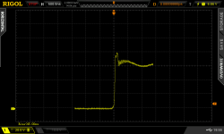
This is a picture of the problem. Notice the big 33V overshoot at turn off on the drain to source scope shot. Also not the dip on the gate to source connection. This was done with no gate to source capacitor installed. I saw this same type of dip on the gate source trace of my previous controller build.
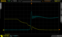
04 g_s_vs_d_s_50ns_off.png

This is what I believe is happening in the above screen shot.
As the MOSFET turns off, the current it was conducting has no where to go, so the voltage shoots up from this high current reacting with the parasitic inductance in the circuit. Since the current was stopped, the magnetic field starts to collapse. A collapsing magnetic field switches to the opposite polarity of what charged it. The D-S connection now has it's parasitic D-S capacitor (Cgd) pulled negative very quickly which causes the G-S (Cgs) parasitic capacitor to discharge and revesre. The G-S becomes fully discharged which shuts off the current flow D-S. The gate to source was already transitioning through the trans conductance region and RDSon is quickly headed towards becoming very high impedance which causes the D-S spike to reverse direction and head back towards the bus voltage. The parasitic Cds and respective Cgs and Cgd capacitance's start to reverse their polarity back to the state they were originally in and charge up again (from being negative), the Cds capacitor rises as it get pulled back to bus voltage. The parasitic inductance in the leads and components add to this as it's field collapses as it switches back polarity as well. Since the MOSFET is now high impedance, the magnetic field has no where to go so the process repeats, but at a lower magnitude. This is seen as ringing after the initial spike. The turn off spike can only last from the time Vds crosses Vbus to the time Vgs reaches the Vgsth threshold which I have previously measured at around 3.4v. This is within the spec sheet value of 3-5V for Vgsth. The reason it can only go back to Vgsth is the circuit has now been shut off and no more energy can enter, only the residual energy within the parasitics are left and they dissipate over the next few micro seconds as ringing dampened only by the parasitic resistance.

Now enter external the gate to source capacitor. All the above still happens, but when Vgs tries to reverse, there is additional capacitance which has been added. This extra capacitance takes longer to discharge which helps prevent the spike because the gate voltage is kept up by the capacitor which resisting the polarity change that tries to happen as the magnetic field collapses and increases the Cgs discharge time. As can be seen in the below screen shot, a polarity change does happen driving Vgs lower for about 200ns, but it's much less than previously seen since it takes more time to discharge the additional capacitor. The previous 36v spike above Vbus is now limited to ~16 volts.

Turn off shot after a 280A on pulse, a single 68nF capacitor was added to a central connection point of the gate & source pins for all 3 MOSFETs.
10 g_s_vs_d_s_200ns_off.png

Comparison of Vgs using a 68nF (purple trace) and 0nF (orange trace)
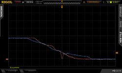
15 0nf_vs_68nf_gs_200ns_off.png

Comparison of Vds using 68nF (white trace) and 0nF (green trace)
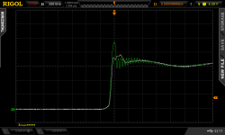
16 0nf_vs_68nf_ds_200ns_off.png


Benefits
1. Reduces turn off overshoot allowing a higher maximum voltage rating due to the extra head room
2. Stretches and flattens out turn off overshoot which reduces RFI
3. Produces less ringing at turn on/off
4. Allows the switching speeds to be pushed faster while maintaining a clean waveform.

Negatives
1. It can require a more powerful gate driver to switch on effectively than would otherwise be required for the given gate charge.
2. If a Miller clamp is not used, this capacitor could be charged up over time by stray inductance leading to the MOSFET Vgsth being reached and turning on causing a shoot through event.
3. Has a small effect on the Miller charge causing longer switch times.

The common method to stop a drain to source turn off spike and subsequent ringing is to increase the gate resistor slowing down the turn off time. The sharp turn off spike also means more emitted RFI, lower maximum bus voltage with regard to part rating, higher switching losses and reduced operating power. Adding external gate to source capacitance appears to improve all of the these issues substantially.

Now on to the Miller clamp feature.

Scoped the opposite gate drive to the one I was firing. I first did it without any power so the Miller clamp was disabled. Discharging ~500A
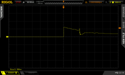
25 g_s_no_miller_clamp_50us.png

This is a zoomed in shot showing the wave form. Voltage creeps up to 0.6 volts when discharging ~500A
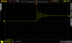
24 g_s_no_miller_clamp_1us.png

Gate driver powered, Miller clamp turned on, the voltage is significantly reduced when discharging ~500A
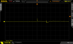
26 g_s_miller_clamp_50us.png

About half of the spike is probably CMRR as I did check it, but didn't get a scope shot. There was certainly some present, about 0.25V worth.
 
its really incredible how far you have come in a year. i've stopped tutoring you a few months ago on this gate driver stuff and you have progressed a mile since then. you're almost ready for the advanced stuff :)

my only comment for the above discussion is that i would accept more ringing than you would with lower G/S cap (67nF is a lot). to eliminate ALL the ringing is not natural and might cause more harm then good. but "harm" i'm talking slight harm since you are in the fine tuning stages of the design there is only small differences as you add/subtract values.
 
Thanks for reviewing my write up. I just used logic along with bits of theory I've read about. I have started to learn the physical structure of the silicon as well. I keep looking for more information for the questions I come up with but it's hard to find. I could not find anything on the cause of ringing after turn on (happens after the Miller Plateau) and as it turns off as I tried to describe above.

Maybe you can answer this next question for me. You said you could tolerate more ringing than I have in my screen shots, how much is OK and how much is too much. Where do I draw the line? My only point of reference is my previous design and my notes from building and tuning it. I've gone back and looked at the screen shots / bench tuning notes many times as my reference.

This design seems like it is way better than my first one and I have a few changes I'll make on the next one which will further reduce noise. I thought up a really slick laminated bus bar system that can handle way more than this design, has full overlap except for the MOSFET leg connection and is easy to manufacture and install by hand. The bus bars on this design were a PITA to install.

I've been asked why I have been testing 500-700A pulses with only 3 MOSFETs in parallel as this controller will never operate at this level. I've been using the high current to test the layout for the future when I try to go for crazy current levels. Trying to get 15-25 parallel devices to play nice together should be a challenge… I don't think anyone knows how many optimised for current sharing parallel MOSFETs can be paralleled before reaching the point of diminished returns.

Since you are my basis for comparison, how difficult is it to get clean looking signals such as the ones above where I am transitioning 300-600A in less than 150ns? If I tolerate a little ringing (probably OK by your standard based on what you said and my previous design) I can drop the gate resistors down from 6.2 on 2.0 off to 4.0 on and 1.5 off which puts my on time at ~90ns and off at ~100ns at 600A. I'm pretty sure that gets my D-S slope would be getting close to the spec sheets 18v/ns max rating where I have to worry about the G-S being charged by the fast dv/dt and getting miller effect turn on. I believe the large G-S cap would help in this are as well.

I have noticed there is a definite line that gets crossed in resistor choice. With a 2.0 off gate resistor I'm OK, with a 1.5 ohm I get some ring and at 1.0 there is more ring than I think would be acceptable.

I am not trying to switch faster and chose the 6.2/2.0 to slow the switching down to 135ns/150ns which still seems really fast.

I've had this controller on the bench for a long time because I was playing around with tuning it and trying to learn how my changes impacted it. I feel a bit relieved now knowing I wasn't wasting my time. There is a lot of physics going on in a single switch event!
 
Back
Top