My new 18 FET TO-247 layout riding video page 10

heathyoung said:
Peak value for acceleration - rather than continuous. With the existing controller I see this for about 8-10 seconds, usually by this time its going fast enough to warrant letting off the throttle!

Pack voltage is 144V, and sags badly to 100V@200A. New batteries will resolve this to about 135-140V @ 200A+.

Continuous is about 12Kw @ 105Kph, worse up hill or into a headwind.

I'm considering building one of these to replace the controller in a Vectrix, the IGBT's are a little temperamental and expensive when they go bad ($500). The takeoff current is nothing too exciting 50A battery side. I think this is due to the phase current limits of the IGBT @ 275A due to current multiplication at low rpm.

I just saw a 2007 Vectrix for sale not to far from me for something like $2400 in working condition. I've been thinking about getting it so I have a street legal platform to continue higher power development on.
 
$2400 is a tad expensive - they do make an interesting platform for development - optical encoder with differential hall outputs, sin/cos outputs. Motor will take 30kw peak without trouble.

Problem is everything is CANBUS - motor controller, body control module, charger - so you have to figure your own dash controls and charger but there is enough space for 90ah of lithium.

Someone was selling the swing arms and motors recently on us ebay.
 
Hi Zombiess

Really enjoying the development of your projects! 8)

Inquiring minds in my small circle wish to know if the power stage be scaled back to a 12-FET by simply not loading the last 6 FETs as opposed to shrinking/redesigning the pcb? We don’t need all that power for our dyno project, although we still want to dabble with the tech and learn.

Thanks, KF
 
hey Zombiess,
ive been looking at designing my own but your look like a very nice and well layed out design.
i would love to use you design and modify it to work with 200v battery 100-200 amps.
cheers
 
bradleyk said:
hey Zombiess,
ive been looking at designing my own but your look like a very nice and well layed out design.
i would love to use you design and modify it to work with 200v battery 100-200 amps.
cheers

That can be done, but my bus bar config is not optimal since it does not fully overlap. I have a fix I designed for it but have yet to have it made. Need to get some copper cut on a water jet.

Im not sure how "robust" this layout is. I have been slacking off on this project (getting busy with others). I have done some pules testing and it looks good but I need more data.
 
I have a golden motor controller apart that is similar to that.
 
Arlo, could you open a topic with photos of that controller? Thanks
 
zombiess said:
I did some testing of the current my gate driver can deliver. Setup is as follows.

I setup a 104mOhm shunt (10x 1.0 ohm resistors) in parallel with the gate drive output hooked up to a 1.0uF snubber cap. The boost stage has 2 10uF caps in parallel feeding it. The 1.0uF cap was used because it was handy and low enough ESR to get a high peak current. I need to parallel several small caps to see how quickly the current can rise. With a 0.1 Ohm gate resistor I managed 14.4A out in 570nS and 13.6A drained from the gate in 960nS which doesn't seem too bad for a giant capacitive load. Now I have some idea about the current rise rate (still needs more testing for rise time). It's no IXYS IXD-614 for speed, but it has some kick ass safety features integrated vs just being a bare gate driver.

On (purple trace is current and is channel B which is my math function.

View attachment 1


I had a look over the circuits and have some questions / thoughts.


Why did you put the DC/DC on a seperate sheet?
Where you thinking of making a DC/DC?


Why have the Gplane connector?
If its for support .. just leave it nc.
REduce chance off current loops.

No cap on Vref pin?

Digital On input from brain could have 100ohm terminator to 0V before the 330R and small cap.
To stop opto false triggering.... but there is filtering on the isolated side and in the TD350.
Parts could be there just nor fitted.

Fault signal protection of opto output?

Why are the td350 NC 4,6 pins conneceted to common?

Why did you choose boosy with emitters linked?

Will Ron/off (R22) get much hotter than Roff r26 and Diode d14??

Clamp circuit has a very long path. Do you see pulses on the Gate signal?
Gate damping cap .. will see lots of pulse currents ... is the type for this.
But it is so far from gate and via 0R5 res's that it wont see the Ccg currents from dV/dt
causing Vcg effects that the clamp is to protect for.

The Zetex Clamp transistor looks very fast on the spec.
Would be interesting to see its Vce signal.

C102 on one phase is linked for mid layer ... but not fitted??
Was mid layer needed ... was it thinner copper??
Why did you link like you did??
It doesn't make sense as a laminated return path.

Too many 90deg corners for me on power flow tracks. chamfers and fillets.

Would yuo be tempted to try to fit a 24 fet into the hammond case.
Your phase boards could fit 4 parallel.

Did you see much overshoot on the FET's

What did the Gate signal look like.
How much delay was there from say the haz side of the opto to turn on/off?

What voltage HV power Caps did you fit?

How did you wire the HASS 600A Current sensors?

Did you get to study the Phase voltage and current on the scope?


These are just some thoughts no need to measure anything.
Just consider them for you next design.

Nice design work Zombiess.
Are you getting good use out of the bike setup?

7C
 
Why did you put the DC/DC on a seperate sheet?
Where you thinking of making a DC/DC?

I'm new to drawing schematics and still learning, just a mistake

Why have the Gplane connector?
If its for support .. just leave it nc.
REduce chance off current loops.

It's for support. I didn't think about the ground loop condition it could possibly create. I didn't know if they should be connected or not, in the end I went with connecting them.

No cap on Vref pin?

Vref is a 5v out supplied by the TD350 for the Coff 2 level shut down timing RC circuit. Manufacturers spec sheet and app notes make no mention of this. It's had already been proven to work in previous designs so I didn't think about it.

Digital On input from brain could have 100ohm terminator to 0V before the 330R and small cap.
To stop opto false triggering.... but there is filtering on the isolated side and in the TD350.
Parts could be there just nor fitted.

Fault signal protection of opto output?

You'll need to clarify what you mean, I don't understand.

Why are the td350 NC 4,6 pins conneceted to common?
It's been advised to me more than once to not leave floating pins (even the NC ones as long as internal connections are verified) on a gate driver due to chances of injecting noise into the chip. I know from some past work that RF can creep around and throw wrenches into things.

Why did you choose boost with emitters linked?
Boost needs to be linked so that 47ohm resistor allows triggering the 2 level turn off function (happens on every pulse, not just fault). Without this resistor in place and the emitters not linked, 2 level turn off does not work (HH and I discovered this on my first build). He had previously designed with this chip, but not with a boost stage which I wanted to add so I could have a gate driver capable of driving many parallel MOSFETs with high Qg. Basically the boost stage exists for the sake of practice in this design.

Will Ron/off (R22) get much hotter than Roff r26 and Diode d14??

Those resistor values were changed on the bench, but no, the power dissipation is not high enough. Resistors are 2512 1W rated. I was taught to oversize the gate resistors to help minimize self heating issues and having values change during operation. Diode is 1A continuous rated but has a Surge Overload Rating to 35A. I'm using in pulse application with a turn off limiting resistor. I think I have a 4.7 ohm on Toff so 3.19A peak off current which only lasts for a few nS before it decays over ~1000nS G-S off time. On was changed to a 10ohm I think, have to look at the boards and then update the schematic. With 10ohm that's a peak of 1.5A worst case. Bench testing with a thermocouple showed it stayed cool as expected based on the math.

Irms_ON = i_peak * Square_root(tp*freq/3)
I have a spreadsheet I created to simplify the gate driver math including the voltage drops of diodes and boost stages. I don't have the exact figure for your but that resistor is dissipating < 250mW based on the RMS current it's seeing and it's a 1W rated resistor.

Clamp circuit has a very long path. Do you see pulses on the Gate signal?

Haven't seen any in single/double pulse testing with 300A pulses triggered by this driver into an air coil from a 95V capacitor bank.


Gate damping cap .. will see lots of pulse currents ... is the type for this.

Not sure if it needs to be. I used an NP0 type to minimize the recharge effect of XR7 and lower rated caps. I do not know how much current this capacitor is seeing, I haven't figured out PSpice yet. A single G-S cap really cleans up turn off overshoot that happens at low bus voltage where the spike (not ringing) can be 2x v_bus. At > 75V bus the turn off spike with no cap is only about 8v, vs 24v buss the spike is ~48v. Not sure what's happening here with the physics and couldn't find anyone with an answer.

But it is so far from gate and via 0R5 res's that it wont see the Ccg currents from dV/dt
causing Vcg effects that the clamp is to protect for.

you lost me

The Zetex Clamp transistor looks very fast on the spec.
Would be interesting to see its Vce signal.

I chose it based on current/voltage/speed since it's marketed as a totem pole gate driver.

C102 on one phase is linked for mid layer ... but not fitted??
Was mid layer needed ... was it thinner copper??
Lots of stuff was added on here for experimenting and several things ended up not being populated. I was experimenting with multiple smaller G-S caps vs 1 large G-S cap, same with G-S pull down resistors.

Why did you link like you did??
It doesn't make sense as a laminated return path.

Trying to shield EMI from the power pass since I had not figured out how to do a laminated buss on this layout. Now I know how to do the laminated buss on this same style layout. Experimenting.

Too many 90deg corners for me on power flow tracks. chamfers and fillets.
I've seen this debated several times with no hard data to back either argument, not at these low frequencies.

Would you be tempted to try to fit a 24 fet into the hammond case.
Your phase boards could fit 4 parallel.

Yup, the more the merrier. I wanted to start at 3, but this case is only good for 4. I'm eventually planning to scale way out with parallel devices. All my builds have the FETS miller plateaus matched.

Did you see much overshoot on the FET's

What did the Gate signal look like.
How much delay was there from say the haz side of the opto to turn on/off?

Need to test

What voltage HV power Caps did you fit?
Kemet C4AE series, 600V
How did you wire the HASS 600A Current sensors?
They will be looped over the output wires, going to be tight, if it even fits, might need a smaller sensor.

Did you get to study the Phase voltage and current on the scope?
nope.

Are you getting good use out of the bike setup?

Not any more, I never ride due to being in too much pain.
 
Alan B said:
zombiess said:
...

Not any more, I never ride due to being in too much pain.

Would a recumbent work for you? Some have really excellent ergo riding positions.

No place to ride, no one to ride with. If I had someone local to me that was into this I'd probably go riding again, pain or not. Riding along at 10mph isn't the kind of riding I prefer. It was fun when I could commute by bike.
 
Back at it tonight. Did some testing of the gate drivers to verify operation, the got brave and tested desaturation detection. Good thing I did too because it turns out my zener needs to be changed out. I hit just over 1000A (dead short) through 3 parallel IRFP4568's on a 200uS pulse and the desat voltage only made it to 6.8V and needs to be a 7.2v by 750A. With a 5uH coil a 200uS pulse with several caps in parallel with the 62v supply it reaches 760A. I decided to do the dead short test just to see how much of a difference it would make and it went to just over 1000A. This was impressive to experience.

I also did a quick load test at 19khz with the 5uH coil for 2-3 seconds at 5% duty cycle. Wow that coil was putting off a strong magnetic field. Made my screw driver feel like it was moving around in sludge.

There really wasn't a whole lot of purpose to most of this other than playing around and verifying some things before I hook it up and try to run a motor. I wasn't worried about the MOSFETs since I have 3 IRFP4568's in parallel and they are on a huge heat sink. I'm withing the operating range of the 3 in parallel, but not by much. I limited the pulse to 1 every 3 seconds.

Current was measured with a 0.375 mOhm shunt and my scope using the math function.

I guess I'll be doing a little soldering re work tomorrow so my desat works as I expect it.

Just an FYI, I didn't just jump right in and put hundreds of amps into my setup, I worked my way up slowly while monitoring the desat trigger and current.
 
I'm glad I did the bench test verification. I now know I need to increase my desat zener diode to 5.6v from 5.1v. I calculated my desat trip point now and its just over 1200a @ Tj=25c. At Tj=125c the desat point drops down to 585 amps. So because my controller is cold, the desat point is way high as I expected. After measuring the real diode voltage drops at 250uA I remembered my blocking diode vf of 1.2 was all wrong. It's 1.2v with 1.0a going through it. With 250uA its only about a 0.48v drop. I forgot to include this in my spreadsheet I use back when I figured it out on my first build.

I am planning to push the limits with this controller if I can. A 10 sec burst rating could be quite high compared to steady state use. It fits the criteria I have for this controller which is not being designed for high current continuous use. I'm going to guesstimate my 30 min continuous use at 100a RMS (141a peak).
 
zombiess said:
I'm glad I did the bench test verification. I now know I need to increase my desat zener diode to 5.6v from 5.1v. I calculated my desat trip point now and its just over 1200a @ Tj=25c. At Tj=125c the desat point drops down to 585 amps. So because my controller is cold, the desat point is way high as I expected. After measuring the real diode voltage drops at 250uA I remembered my blocking diode vf of 1.2 was all wrong. It's 1.2v with 1.0a going through it. With 250uA its only about a 0.48v drop. I forgot to include this in my spreadsheet I use back when I figured it out on my first build.

I am planning to push the limits with this controller if I can. A 10 sec burst rating could be quite high compared to steady state use. It fits the criteria I have for this controller which is not being designed for high current continuous use. I'm going to guesstimate my 30 min continuous use at 100a RMS (141a peak).


Using this type of circuit for current control may actually be fast enough to run the silicon at it's thermal limits. I realize It's a miracle safety feature that prevents needing to rebuild/replace a power stage after each control glitch. I would think using this type of current control operation as an EV "clutch-dump" effect for bursts of torque, and it could be set for a lower current threshold and not interfere with the existing shoot-through protection circuit you already have, but only activated from some user input that commands it for whatever duration of time it safely can. I would think your setup could easily do 1500A for >0.5seconds if it was starting from room temperature. Even after a motor saturates it still contributes additional torque per amp for a bit, might as well use it for launching.

For EV drag applications, it would naturally increase the current limits while the dice remained cooler if you pre-chilled the assembly with LN2 or a CO2 extinguisher before launching. The Silicon itself and the grids of copper current collectors have some thermal mass, if you started from very cold, that time seems it would be long enough to act like a clutch dump.
 
Be careful some of the data sheets show reduced current at -30 - -40 degC
 
if you pre-chilled the assembly with LN2 or a CO2 extinguisher before launching
lol, i've actually done that. in a temperature controlled room that uses LN2 to reach whatever temp you wanted. i dropped to -40C then i hit the max current. what i learned is that although the max current was not an issue (designed intentionally that way, no burst capability), what WAS a problem was the rate of change of temperature within the die. inside the mosfet is maybe 4 or 5 different types of metals, all bonding together. they each have a different thermal rate of contraction/expansion. of course it is a lot of effort to make sure no one interface has a large difference, but, when you stress like i did you can reveal the weakness.

IXYS IGBT never had such a weakness.
SEMIKRON never had such a weakness
IRF = complete fail.
Microsemi = marginal (only a few fail, most pass)

hey, they all have the same name "mosfet" or "IGBT" but they not built all the same.
 
liveforphysics said:
Using this type of circuit for current control may actually be fast enough to run the silicon at it's thermal limits. I realize It's a miracle safety feature that prevents needing to rebuild/replace a power stage after each control glitch. I would think using this type of current control operation as an EV "clutch-dump" effect for bursts of torque, and it could be set for a lower current threshold and not interfere with the existing shoot-through protection circuit you already have, but only activated from some user input that commands it for whatever duration of time it safely can. I would think your setup could easily do 1500A for >0.5seconds if it was starting from room temperature. Even after a motor saturates it still contributes additional torque per amp for a bit, might as well use it for launching.

Funny you mention this. When I was testing the other day I was thinking of monitoring the RDSon value to estimate Tj so that I could set a safety margin of say 10-25% under the 175c die temp max, then let the controller run the silicon to that limit. What's really cool is this method would allow it to track and automatically scale back as the die temperature goes up. For continuous use the legs are often the limiting factor on modern high current parts. I'm going to add this to my idea list.

They key to this working is making sure the parallel MOSFETs current share VERY well, but I think I have that part figured out.
 
Took some video of the setup during bench testing. Tweaked the desat detection so it triggers around 750A. If the current rise is fast due to the inductive load being very low.

Pretty happy with the setup. I sent lots of +600A 200uS pulses into my test setup at 44V and monitored the gate drive signal and also the D-S turn on signal. I'm seeing 200nS switching times D-S and 1300nS 0-10V on the G-S. I'd like to speed up the 0-10V G-S time, but I'm concerned with the current levels it might start to ring. It would be nice to see < 1000nS G-S switch times. I might drop my turn on resistor from 10 ohms down to 7 ohms and see what happens since everything looks clean right now. No ringing, no noise, not even with my non optimal probe config. Part of this is most likely due to switching on the slower switching, but I'd like to think my layout is the biggest factor.

First up is a reference picture from my very first design, a 24 MOSFET IRFB4115 controller which has run great in all testing so far.

This is a 95A pulse done a 62v while measuring Gate to Source. Doesn't look too bad and has worked well in operation so far.
g_s_on_62v_95a.png

These are from the 18 FET IRFP4568 controller I'm now playing with.


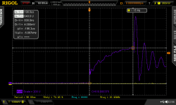
This is the math function measuring the voltage across a 0.000375 ohm shunt (value verified with a 6.5 digit dmm). Bus voltage was 42v and produces a 640A pulse into the 5uH load coil (about 4mOhm) in the 200uS pulse period. That huge ring after the driver shuts off on the purple trace measuring the shunt current into the load coil changes drastically in amplitude depending on the probe lead orientation so I'm guessing it's just noise being picked up by the probe lead wire since I am pumping out a little EM field with my inductor. The current trace before it shuts off always looks the same no matter the probe wires orientation.
18fet_640a_shunt.png

This is the Gate to Source wave form from the gate driver while triggering the 640A pulse, doesn't look like it's even working hard.
18fet_g_s_on_640amps.png

Same as above, but zoomed out to show any ringing
18fet_g_s_on_640amps2.png

This is what the turn off of the gate drive looks like
18fet_g_s_off_640amps.png

To achieve the super high currents I have 4 1000uF low ESR caps in parallel with the power supply. The controller also has 60uF of PP DC Link caps rated for very high peak currents and also 3uF of PP snubber caps. The short circuit current is impressive. Had a little fun using some thin wire (probably 20 gauge) and watching the pretty spark as it vaporized.

I started to question if my math was correct when I was seeing such high currents, but after playing around with the controller for about 45 mins dumping 500-800A 200uS pulses through it every 3 seconds I noticed the heat sink it was mounted to was just barely warm to the touch, normally it feels cold.
 
zombiess said:
When I was testing the other day I was thinking of monitoring the RDSon value to estimate Tj so that I could set a safety margin of say 10-25% under the 175c die temp max, then let the controller run the silicon to that limit.

There's another method, I've been wanting to do this for some time on a FET switch test fixture. I haven't given it much thought, so I don't know what would be easier to implement. The other method is to monitor the parasitic diode forward voltage drop, which is proportional to die temperature, almost linearly up to some 100ºC, then less.
 
This is the math function measuring the voltage across a 0.000375 ohm shunt
your math function probably does not know how to deal with a transient. i would not trust that result.

but keep in mind that the transient is probably real and it is this "noise" as well as rapidly changing reference that will mess with any circuitry you want to build to detect temp rise via Rds_on or diode voltage drop. i'll come back to this topic later when i have more free time. busy now with other project you're well aware of.
 
It would be interesting to see if you can creep up towards the data sheet realm of values with respect to pulse currents. If any setup is going to do it, it would be one that used highhopes techniques.
 
HighHopes said:
This is the math function measuring the voltage across a 0.000375 ohm shunt
your math function probably does not know how to deal with a transient. i would not trust that result.

but keep in mind that the transient is probably real and it is this "noise" as well as rapidly changing reference that will mess with any circuitry you want to build to detect temp rise via Rds_on or diode voltage drop. i'll come back to this topic later when i have more free time. busy now with other project you're well aware of.

Curious to hear your thoughts on the scope math function. The math function is not good for real time for sure, but I was measuring every 3 seconds and I made sure I had the volts/div set with enough resolution to capture good detail. The math function would get blocky as one expects if the resolution sucks.

The only funky thing I saw the math function do was when I tried doing some fast stuff at 19khz. It had some wonky results at times which didn't really surprise me. I verified the current against the captured wave form, it's not 100%, but it's pretty close so you are correct it's missing transients, but it's close enough to show there is a lot of current flowing :)
 
Back
Top